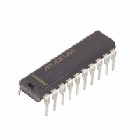
MAX147BCPP+ Maxim Integrated Products, MAX147BCPP+ Datasheet - Page 3

MAX147BCPP+
Manufacturer Part Number
MAX147BCPP+
Description
IC SRL ADC 8CH 12BIT 2.7V 20-DIP
Manufacturer
Maxim Integrated Products
Datasheet
1.MAX147BCAP.pdf
(24 pages)
Specifications of MAX147BCPP+
Number Of Bits
12
Sampling Rate (per Second)
133k
Data Interface
MICROWIRE™, QSPI™, Serial, SPI™
Number Of Converters
1
Power Dissipation (max)
889mW
Voltage Supply Source
Single Supply
Operating Temperature
0°C ~ 70°C
Mounting Type
Through Hole
Package / Case
20-DIP (0.300", 7.62mm)
Architecture
SAR
Conversion Rate
133 KSPs
Resolution
12 bit
Input Type
Voltage
Interface Type
4-Wire (SPI, QSPI, MICROWIRE, TMS320)
Voltage Reference
Internal 2.5 V or External
Supply Voltage (max)
5.25 V
Supply Voltage (min)
2.7 V
Maximum Power Dissipation
889 mW
Maximum Operating Temperature
+ 70 C
Mounting Style
Through Hole
Minimum Operating Temperature
0 C
Lead Free Status / RoHS Status
Lead free / RoHS Compliant
ELECTRICAL CHARACTERISTICS (continued)
(V
clocks/conversion cycle (133ksps); MAX146—4.7µF capacitor at VREF pin; MAX147—external reference, VREF = 2.500 V applied to
VREF pin; T
Track/Hold Acquisition Time
Aperture Delay
Aperture Jitter
Internal Clock Frequency
External Clock Frequency
Input Voltage Range, Single-
Ended and Differential (Note 6)
Multiplexer Leakage Current
Input Capacitance
VREF Output Voltage
VREF Short-Circuit Current
VREF Temperature Coefficient
Load Regulation (Note 7)
Capacitive Bypass at VREF
Capacitive Bypass at REFADJ
REFADJ Adjustment Range
VREF Input Voltage Range
(Note 8)
VREF Input Current
VREF Input Resistance
Shutdown VREF Input Current
REFADJ Buffer Disable Threshold
Capacitive Bypass at VREF
Reference Buffer Gain
REFADJ Input Current
ANALOG/COM INPUTS
INTERNAL REFERENCE (MAX146 only, reference buffer enabled)
EXTERNAL REFERENCE AT VREF (Buffer disabled)
EXTERNAL REFERENCE AT REFADJ
DD
= +2.7V to +3.6V (MAX146); V
PARAMETER
A
= T
MIN
to T
_______________________________________________________________________________________
MAX
; unless otherwise noted.)
DD
SYMBOL
= +2.7V to +5.25V (MAX147); COM = 0; f
t
ACQ
SHDN = FLOAT
SHDN = V
Data transfer only
Unipolar, COM = 0V
Bipolar, COM = VREF / 2
On/off leakage current, V
T
MAX146_C
MAX146_E
MAX146_M
0 to 0.2mA output load
Internal compensation mode
External compensation mode
VREF = 2.5V
Internal compensation mode
External compensation mode
MAX146
MAX147
MAX146
MAX147
A
+2.7V, Low-Power, 8-Channel,
= +25°C
DD
CONDITIONS
CH_
= 0V or V
SCLK
Serial 12-Bit ADCs
= 2.0MHz; external clock (50% duty cycle); 15
DD
2.480
0.047
V
MIN
0.1
4.7
1.0
0.5
4.7
DD
18
0
0
0
-
0.225
±0.01
2.500
TYP
0.35
±1.5
0.01
2.06
2.00
<50
±30
±30
±30
100
1.8
30
16
25
±VREF / 2
0 to VREF
V
50mV
2.520
MAX
±50
±60
±80
DD
±50
±10
150
1.5
2.0
2.0
±1
30
10
+
ppm/°C
UNITS
MHz
MHz
mA
mV
V/V
µA
pF
µA
kΩ
µA
µA
µs
ns
ps
µF
µF
µF
%
V
V
V
V
3


