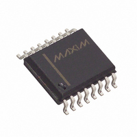
MAX194BCWE+T Maxim Integrated Products, MAX194BCWE+T Datasheet - Page 16

MAX194BCWE+T
Manufacturer Part Number
MAX194BCWE+T
Description
IC ADC 14BIT 85KSPS 16-SOIC
Manufacturer
Maxim Integrated Products
Datasheet
1.MAX194BEWE.pdf
(24 pages)
Specifications of MAX194BCWE+T
Number Of Bits
14
Sampling Rate (per Second)
85k
Data Interface
QSPI™, Serial, SPI™
Number Of Converters
1
Power Dissipation (max)
80mW
Voltage Supply Source
Analog and Digital, Dual ±
Operating Temperature
0°C ~ 70°C
Mounting Type
Surface Mount
Package / Case
16-SOIC (0.300", 7.50mm Width)
Lead Free Status / RoHS Status
Lead free / RoHS Compliant
If DC accuracy is important, choose a buffer with an
offset much less than the MAX194’s maximum offset
(±1 LSB = ±488µV for a ±4V input range), or whose off-
set can be trimmed while maintaining good stability
over the required temperature range.
Figure 14 shows a good circuit for DC and low-frequen-
cy use. The MAX400 has very low offset (10µV) and
drift (0.2µV/°C), and low voltage noise (10nV/ √ Hz) as
well. However, its gain-bandwidth product (GBW) is
much too low to drive AIN directly, so the analog input
is bypassed to present a low impedance at high fre-
quencies. The large bypass capacitor is isolated from
the amplifier output by a 100Ω resistor, which provides
additional noise filtering. Since the ±15V supplies
exceed the AIN range, add protection diodes at AIN.
Figure 15 shows a wide-bandwidth amplifier (MAX427)
driving a wideband video buffer, which is capable of dri-
ving AIN and a small bypass capacitor (for noise reduc-
tion) directly. The video buffer is inside the MAX427’s
feedback loop, providing good DC accuracy, while the
buffer’s low output impedance and high current capabil-
Figure 17. MAX194 Connection to QSPI Processor Clocking
Data Out During Conversions
14-Bit, 85ksps ADC with 10µA Shutdown
16
______________________________________________________________________________________
* THE USE OF THESE SIGNALS ADDS FLEXIBILITY AND FUNCTIONALITY
BUT IS NOT REQUIRED TO IMPLEMENT THE INTERFACE.
QSPI
GPT
PCS0
MISO
*OC3
*OC2
*IC1
SCK
Recommended Circuits
CS
CONV
CLK
DOUT
SCLK
BP/UP/SHDN
EOC
RESET
MAX194
DC Accuracy
ity provide good AC performance. AIN is diode-
clamped to the ±5V rails to prevent overvoltage. The
MAX427’s 15µV maximum offset voltage, 0.8µV/°C maxi-
mum drift, and less than 5nV/ √ Hz noise specifications
make this an excellent choice for AC/DC use.
If ±15V supplies are unavailable, Figure 16’s circuit works
very well with the ±5V analog supplies used by the
MAX194. The MAX410 has a minimum ±3.5V common-
mode input range, with a similar output voltage swing,
which allows use of a reference voltage to 3.5V. The offset
voltage (250µV), drift (1µV/°C), unity-gain bandwidth
(28MHz), and low voltage noise (2.4nV/ √ Hz) are appropri-
ate for 14-bit performance. The 0.01µF bypass capacitor
improves the noise performance.
The two basic interface modes are defined according
to whether serial data is received during the conversion
(clocked with CLK, SCLK unused) or in bursts between
conversions (clocked with SCLK). Each mode is pre-
sented interfaced to a QSPI processor, but is also com-
patible with SPI.
In this mode, each data bit is read from the MAX194 dur-
ing the conversion as it is determined. SCLK is grounded
and CLK is used as both the conversion clock and the
serial data clock. Figure 17 shows a QSPI processor
connected to the MAX194 for use in this mode and
Figure 18 is the associated timing diagram.
In addition to the standard QSPI interface signals, gener-
al I/O lines are used to monitor EOC and to drive
BP/UP/SHDN and RESET. The two general output pins
may not be necessary for a given application and, if I/O
lines are unavailable, the EOC connection can be omit-
ted as well.
The EOC signal is monitored during calibration to deter-
mine when calibration is finished and before beginning
a conversion to ensure the MAX194 is not in mid-con-
version, but it is possible for a system to ignore EOC
completely. On power-up or after pulsing RESET low,
the µP must provide 14,000 CLK cycles to complete the
calibration sequence (Figure 2). One way to do this is
to toggle CLK and monitor EOC until it goes low, but it
is possible to simply count 14,000 CLK cycles to com-
plete the calibration. Similarly, it is unnecessary to
check the status of EOC before beginning a conversion
if you are sure the last conversion is complete. This can
be done by ensuring that every conversion consists of
at least 20 CLK cycles.
Operating Modes and SPI/QSPI Interfaces
Conversion and Data Transfer)
Mode 1 (Simultaneous


