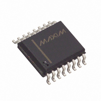
MAX194BCWE+ Maxim Integrated Products, MAX194BCWE+ Datasheet - Page 22

MAX194BCWE+
Manufacturer Part Number
MAX194BCWE+
Description
IC ADC 14BIT 85KSPS SHTDN 16SOIC
Manufacturer
Maxim Integrated Products
Datasheet
1.MAX194BEWE.pdf
(24 pages)
Specifications of MAX194BCWE+
Number Of Bits
14
Sampling Rate (per Second)
85k
Data Interface
QSPI™, Serial, SPI™
Number Of Converters
1
Power Dissipation (max)
80mW
Voltage Supply Source
Analog and Digital, Dual ±
Operating Temperature
0°C ~ 70°C
Mounting Type
Surface Mount
Package / Case
16-SOIC (0.300", 7.50mm Width)
Lead Free Status / RoHS Status
Lead free / RoHS Compliant
Figure 22. Supply Bypassing and Grounding
graph of theoretical power consumption vs. conver-
sions per second for the MAX194 that assumes the
conversion clock is 1.7MHz and the converter is shut
down as much as possible between conversions.
Stop CLK before shutting down the MAX194. CLK must
be stopped without generating short clock pulses. Short
CLK pulses (less than 150ns), or shutting down the
MAX194 without stopping CLK, may adversely affect the
MAX194’s internal calibration data. In applications
where CLK is free-running and asynchronous, use the
circuit of Figure 24 to stop CLK cleanly.
To minimize the time required to settle and perform a
conversion, shut the converter down only after a con-
version is finished and the desired mode (unipolar or
bipolar) has been set. This ensures that the sampling
capacitor array is properly connected to the input sig-
nal. If shut down in mid-conversion, when awakened,
the MAX194 finishes the old conversion, allows four
clock (CLK) cycles for input acquisition, then begins
the new conversion.
High-speed sampling capability, 85ksps throughput,
and wide dynamic range make the MAX194 ideal for
AC applications and signal processing. To support
these and other related applications, Fast Fourier
Transform (FFT) test techniques are used to guarantee
the ADC’s dynamic frequency response, distortion, and
noise at the rated throughput. Specifically, this involves
14-Bit, 85ksps ADC with 10µA Shutdown
22
_____________Dynamic Performance
______________________________________________________________________________________
5V
5V
10 F
10 F
10
10
10 F
10 F
0.1 F
0.1 F
0.1 F
0.1 F
VDDD
VDDA
DGND
AGND
VSSA
VSSD
MAX194
applying a low-distortion sine wave to the ADC input
and recording the digital conversion results for a
specified time. The data is then analyzed using an FFT
algorithm, which determines its spectral content.
Conversion errors are then seen as spectral elements
other than the fundamental input frequency.
Signal-to-Noise Ratio (SNR) is the ratio between the
RMS amplitude of the fundamental input frequency to
the RMS amplitude of all other ADC output signals. The
output band is limited to frequencies above DC and
below one-half the ADC sample rate. This usually (but
not always) includes distortion as well as noise compo-
nents. For this reason, the ratio is sometimes referred to
as Signal-to-Noise + Distortion (SINAD).
The theoretical minimum ADC noise is caused by quan-
tization error and is a direct result of the ADC’s resolu-
tion: SNR = (6.02N + 1.76)dB, where N is the number
of bits of resolution. A perfect 14-bit ADC can, there-
fore, do no better than 86dB. An FFT plot of the output
shows the output level in various spectral bands. Figure
25 shows the result of sampling a pure 1kHz sinusoid at
85ksps with the MAX194.
By transposing the equation that converts resolution to
SNR, we can, from the measured SNR, determine the
effective resolution or the “effective number of bits” the
ADC provides: N = (SNR - 1.76) / 6.02. Substituting
SINAD for SNR in this formula results in a better
Figure 23. Power Dissipation vs. Conversions/sec When
Shutting the MAX194 Down Between Conversions
0.01
100
0.1
10
1
1
20 s WAKE-UP DELAY
0.05LSB ERROR
10
CONVERSIONS PER SECOND
Signal-to-Noise Ratio and
Effective Number of Bits
100
3.2 s WAKE-UP DELAY
0.1LSB ERROR
1000
10,000 100,000


