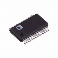
AD9224ARS Analog Devices Inc, AD9224ARS Datasheet - Page 4

AD9224ARS
Manufacturer Part Number
AD9224ARS
Description
IC ADC 12BIT 40MSPS 28-SSOP
Manufacturer
Analog Devices Inc
Datasheet
1.AD9224ARSZRL.pdf
(24 pages)
Specifications of AD9224ARS
Rohs Status
RoHS non-compliant
Number Of Bits
12
Sampling Rate (per Second)
40M
Data Interface
Parallel
Number Of Converters
7
Power Dissipation (max)
450mW
Voltage Supply Source
Single Supply
Operating Temperature
-40°C ~ 85°C
Mounting Type
Surface Mount
Package / Case
28-SSOP (0.200", 5.30mm Width)
For Use With
AD9224-EB - BOARD EVAL FOR AD9224
Available stocks
Company
Part Number
Manufacturer
Quantity
Price
Part Number:
AD9224ARS
Manufacturer:
ADI/亚德诺
Quantity:
20 000
Company:
Part Number:
AD9224ARSZ
Manufacturer:
AD
Quantity:
1 600
Part Number:
AD9224ARSZ
Manufacturer:
ADI/亚德诺
Quantity:
20 000
Part Number:
AD9224ARSZRL
Manufacturer:
ADI/亚德诺
Quantity:
20 000
CAUTION
ESD (electrostatic discharge) sensitive device. Electrostatic charges as high as 4000 V readily
accumulate on the human body and test equipment and can discharge without detection.
Although the AD9224 features proprietary ESD protection circuitry, permanent damage may
occur on devices subjected to high energy electrostatic discharges. Therefore, proper ESD
precautions are recommended to avoid performance degradation or loss of functionality.
AD9224
ABSOLUTE MAXIMUM RATINGS*
Pin Name
AVDD
DRVDD
AVSS
AVDD
REFCOM
CLK
Digital Outputs DRVSS
VINA, VINB
VREF
SENSE
CAPB, CAPT
Junction Temperature
Storage Temperature
Lead Temperature (10 sec)
*Stresses above those listed under Absolute Maximum Ratings may cause perma-
Model
AD9224ARS
AD9224-EB
nent damage to the device. This is a stress rating only; functional operation of the
device at these or any other conditions above those indicated in the operational
sections of this specification is not implied. Exposure to absolute maximum
ratings for extended periods may affect device reliability.
ANALOG
OUTPUT
CLOCK
INPUT
INPUT
DATA
S1
t
CH
With
Respect to Min
AVSS
DRVSS
DRVSS
DRVDD
AVSS
AVSS
AVSS
AVSS
AVSS
AVSS
Figure 1. Timing Diagram
t
C
t
CL
S2
Temperature Range
–40 C to +85 C
–0.3
–0.3
–0.3
–6.5
–0.3
–0.3
–0.3
–0.3
–0.3
–0.3
–0.3
–65
S3
Max
+6.5
+6.5
+0.3
+6.5
+0.3
AVDD + 0.3
DRVDD + 0.3
AVDD + 0.3
AVDD + 0.3
AVDD + 0.3
AVDD + 0.3
+150
+150
+300
S4
t
OD
DATA 1
ORDERING GUIDE
Units
V
V
V
V
V
V
V
V
V
V
V
C
C
C
Package Description
28-Lead Shrink Small Outline (SSOP)
Evaluation Board
–4–
Pin
Number
1
2
3–12
13
14
15, 26
16, 25
17
18
19
20
21
22
23
24
27
28
Name
CLK
BIT 12
BIT 11–2
BIT 1
OTR
AVDD
AVSS
SENSE
VREF
REFCOM
CAPB
CAPT
CML
VINA
VINB
DRVSS
DRVDD
PIN FUNCTION DESCRIPTIONS
(AVSS)
(LSB) BIT 12
(MSB) BIT 1
BIT 11
BIT 10
PIN CONFIGURATION
BIT 9
BIT 8
BIT 7
BIT 6
BIT 5
BIT 4
BIT 3
BIT 2
CLK
OTR
28-Lead SSOP
10
11
12
13
14
1
2
3
4
5
6
7
8
9
Description
Clock Input Pin
Least Significant Data Bit (LSB)
Data Output Bit
Most Significant Data Bit (MSB)
Out of Range
+5 V Analog Supply
Analog Ground
Reference Select
Input Span Select (Reference I/O)
Reference Common
Noise Reduction Pin
Noise Reduction Pin
Common-Mode Level (Midsupply)
Analog Input Pin (+)
Analog Input Pin (–)
Digital Output Driver Ground
+3 V to +5 V Digital Output
Driver Supply
(Not to Scale)
TOP VIEW
AD9224
WARNING!
28
27
26
25
24
23
22
21
20
19
18
17
16
15
DRVDD
DRVSS
AVDD
AVSS
VINB
VINA
CML
CAPT
CAPB
REFCOM (AVSS)
VREF
SENSE
AVSS
AVDD
Package Option
RS-28
ESD SENSITIVE DEVICE
REV. A


