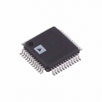
AD7660AST Analog Devices Inc, AD7660AST Datasheet - Page 17

AD7660AST
Manufacturer Part Number
AD7660AST
Description
IC ADC 16BIT UNIPOLAR 48-LQFP
Manufacturer
Analog Devices Inc
Series
PulSAR®r
Datasheet
1.AD7660ASTZRL.pdf
(20 pages)
Specifications of AD7660AST
Rohs Status
RoHS non-compliant
Number Of Bits
16
Sampling Rate (per Second)
100k
Data Interface
Serial, Parallel
Number Of Converters
1
Power Dissipation (max)
25mW
Voltage Supply Source
Analog and Digital
Operating Temperature
-40°C ~ 85°C
Mounting Type
Surface Mount
Package / Case
48-LQFP
For Use With
EVAL-AD7660CBZ - BOARD EVALUATION FOR AD7660
Available stocks
Company
Part Number
Manufacturer
Quantity
Price
Company:
Part Number:
AD7660AST
Manufacturer:
BROADCOM
Quantity:
27
Company:
Part Number:
AD7660AST
Manufacturer:
ADI
Quantity:
300
Company:
Part Number:
AD7660ASTZ
Manufacturer:
ATMEL
Quantity:
36
Company:
Part Number:
AD7660ASTZ
Manufacturer:
ADI
Quantity:
246
Company:
Part Number:
AD7660ASTZ
Manufacturer:
Analog Devices Inc
Quantity:
10 000
Part Number:
AD7660ASTZ
Manufacturer:
ADI/亚德诺
Quantity:
20 000
Company:
Part Number:
AD7660ASTZRL
Manufacturer:
Analog Devices Inc
Quantity:
10 000
External Clock Data Read during Conversion
Figure 20 shows the detailed timing diagrams of this method.
During a conversion, while both CS and RD are LOW, the
result of the previous conversion can be read. The data is shifted
out, MSB first, with 16 clock pulses, and is valid on both the
rising and falling edges of the clock. The 16 bits have to be read
before the current conversion is complete; this, otherwise,
RDERROR is pulsed HIGH and can be used to interrupt the host
interface to prevent incomplete data reading. There is no daisy-
chain feature in this mode, and RDC/SDIN input should always
be tied either HIGH or LOW.
To reduce performance degradation due to digital activity, a fast
discontinuous clock of at least 18 MHz is recommended to ensure
that all the bits are read during the first half of the conversion
phase. For this reason, this mode is more difficult to use.
MICROPROCESSOR INTERFACING
The AD7660 is ideally suited for traditional dc measurement
applications supporting a microprocessor, and for ac signal pro-
cessing applications interfacing to a digital signal processor.
The AD7660 is designed to interface either with a parallel 8-bit or
16-bit wide interface, or with a general-purpose serial port or I/O
ports on a microcontroller. A variety of external buffers can be
used with the AD7660 to prevent digital noise from coupling
into the ADC. The following section discusses the use of an
AD7660 with an ADSP-219x SPI equipped DSP.
REV. D
Figure 20. Slave Serial Data Timing for Reading (Read Previous Conversion during Convert)
SDOUT
CNVST
BUSY
SCLK
CS
t
16
t
3
t
31
X
t
36
1
t
35
D15
t
37
2
D14
t
EXT/INT = 1
32
3
D13
–17–
SPI Interface (ADSP-219x)
Figure 21 shows an interface diagram between the AD7660 and
an SPI-equipped ADSP-219x. To accommodate the slower
speed of the DSP, the AD7660 acts as a slave device and data
must be read after conversion. This mode also allows the daisy-
chain feature. The convert command can be initiated in response
to an internal timer interrupt. The reading process cab be initi-
ated in response to the end-of-conversion signal (BUSY going
LOW) using an interrupt line of the DSP. The serial interface
(SPI) on the ADSP-219x is configured for master mode—
(MSTR) = 1, Clock Polarity bit (CPOL) = 0, Clock Phase bit
(CPHA) = 1, and SPI Interrupt Enable (TIMOD) = 00— by
writing to the SPI control register (SPICLTx). To meet all
timing requirements, the SPI clock should be limited to 17
Mbps, which allows it to read an ADC result in less than 1 ms.
When a higher sampling rate is desired, use of one of the paral-
lel interface modes is recommended.
INVSCLK = 0
Figure 21. Interfacing the AD7660 to an SPI Interface
DVDD
14
INVSCLK
RD
SER/PAR
EXT/INT
15
AD7660*
*ADDITIONAL PINS OMITTED FOR CLARITY
D1
16
SDOUT
CNVST
BUSY
SCLK
RD = 0
CS
D0
SPIxSEL (PFx)
MISOx
SCKx
PFx or TFSx
PFx
ADSP-219x*
AD7660


