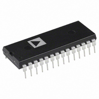
AD7862AN-3 Analog Devices Inc, AD7862AN-3 Datasheet - Page 9

AD7862AN-3
Manufacturer Part Number
AD7862AN-3
Description
IC ADC 12BIT DUAL 250KSPS 28-DIP
Manufacturer
Analog Devices Inc
Datasheet
1.AD7862ARZ-10.pdf
(16 pages)
Specifications of AD7862AN-3
Rohs Status
RoHS non-compliant
Number Of Bits
12
Sampling Rate (per Second)
250k
Data Interface
Parallel
Number Of Converters
2
Power Dissipation (max)
75mW
Voltage Supply Source
Analog and Digital
Operating Temperature
-40°C ~ 85°C
Mounting Type
Through Hole
Package / Case
28-DIP (0.600", 15.24mm)
and fourth read pulses, after the second conversion and A0 high,
access the result from Channel B (V
state can be changed any time after the CONVST goes high,
i.e., track/holds into hold, and 400 ns prior to the next falling
edge of CONVST. Data is read from the part via a 12-bit
parallel data bus with standard CS and RD signal, i.e., the read
operation consists of a negative going pulse on the CS pin
combined with two negative going pulses on the RD pin (while
the CS is low), accessing the two 12-bit results. Once the read
operation has taken place, a further 300 ns should be allowed
before the next falling edge of CONVST to optimize the settling
of the track/hold amplifier before the next conversion is initiated.
With the internal clock frequency at its maximum (3.7 MHz—not
accessible externally), the achievable throughput rate for the
part is 3.6 s (conversion time) plus 100 ns (read time) plus
0.3 s (acquisition time). This results in a minimum throughput
time of 4 s (equivalent to a throughput rate of 250 kHz).
Read Options
Apart from the read operation described above and displayed in
Figure 5a, other CS and RD combinations can result in
different channels/inputs being read in different combinations.
Suitable combinations are shown in Figures 5b through 5d.
REV. 0
DATA
RD
CS
Figure 5b. Read Option A
CONVST
Figure 5a. Mode 1 Timing Operation Diagram for High Sampling Performance
BUSY
DATA
RD
CS
A0
V
A1
B1
t
and V
CONV
V
t
A2
3
= 3.6µs
B2
respectively). A0’s
t
5
t
1
V
t
4
A1
t
6
V
A2
400ns
t
300ns
2
–9–
OPERATING MODES
Mode 1 Operation (High Sampling Performance)
The timing diagram in Figure 5a is for optimum performance in
operating mode 1 where the falling edge of CONVST starts
conversion and puts the track/hold amplifiers into their hold
mode. This falling edge of CONVST also causes the BUSY
signal to go high to indicate that a conversion is taking place.
The BUSY signal goes low when the conversion is complete,
which is 3.6 s max after the falling edge of CONVST, and new
data from this conversion is available in the output latch of the
AD7862. A read operation accesses this data. If the multiplexer
select A0 is low, the first and second read pulses after the first
conversion access the result from Channel A (V
DATA
RD
CS
A0
DATA
RD
CS
V
B1
Figure 5c. Read Option B
Figure 5d. Read Option C
t
V
7
A1
V
B2
V
A1
V
A2
V
V
A1
A1
AD7862
B1
and V
A2


