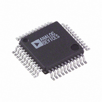
AD7865AS-3 Analog Devices Inc, AD7865AS-3 Datasheet - Page 4

AD7865AS-3
Manufacturer Part Number
AD7865AS-3
Description
IC ADC 14BIT 4CH 5V 44-MQFP
Manufacturer
Analog Devices Inc
Specifications of AD7865AS-3
Rohs Status
RoHS non-compliant
Number Of Bits
14
Sampling Rate (per Second)
350k
Data Interface
Parallel
Number Of Converters
1
Power Dissipation (max)
160mW
Voltage Supply Source
Analog and Digital
Operating Temperature
-40°C ~ 85°C
Mounting Type
Surface Mount
Package / Case
44-MQFP, 44-PQFP
Available stocks
Company
Part Number
Manufacturer
Quantity
Price
Company:
Part Number:
AD7865AS-3
Manufacturer:
AD
Quantity:
1 831
Company:
Part Number:
AD7865AS-3
Manufacturer:
ADI
Quantity:
200
AD7865
TIMING CHARACTERISTICS
Parameter
t
t
t
t
t
t
Read Operation
Write Operation
External Clock
NOTES
1
2
3
4
5
Specifications subject to change without notice.
Sample tested at +25 C to ensure compliance. All input signals are measured with tr = tf = 1 ns (10% to 90% of +5 V) and timed from a voltage level of +1.6 V.
See Figures 6, 7 and 8.
Refer to the Standby Mode Operation section. The MAX specification of 1 s is valid when using a 0.1 F decoupling capacitor on the V
Measured with the load circuit of Figure 1 and defined as the time required for an output to cross 0.8 V or 2.4 V.
These times are derived from the measured time taken by the data outputs to change 0.5 V when loaded with the circuit of Figure 1. The measured number is then
CONV
ACQ
BUSY
WAKE-UP
1
2
extrapolated back to remove the effects of charging or discharging the 50 pF capacitor. This means that the times quoted in the timing characteristics are the true bus
relinquish times of the part and as such are independent of external bus loading capacitances.
t
t
t
t
t
t
t
t
t
t
t
t
t
t
t
t
3
4
5
6
7
8
9
10
11
12
13
14
15
16
17
18
4
5
—External V
REF
3
Figure 1. Load Circuit for Access Time and Bus Relinquish Time
A, B, Y Versions
2.4
3.2
0.35
No. of Channels
1
35
70
0
0
35
35
40
5
30
15
120
180
70
15
0
20
0
0
5
5
200
(t
CONV
1, 2
)
(V
T
TO OUTPUT
MIN
DD
to T
= +5 V
PIN
MAX
Units
ns min
ns min
ns min
ns min
ns min
ns max
ns max
ns min
ns max
ns min
ns min
ns max
ns max
ns max
ns min
ns min
ns min
ns min
ns min
ns min
ns min
s max
s max
s max
s max
s max
unless otherwise noted.)
5%, AGND = DGND = 0 V, V
50pF
–4–
1.6mA
400 A
Test Conditions/Comments
Conversion Time, Internal Clock
Conversion Time, External Clock (5 MHz)
Acquisition Time
Selected Number of Channels Multiplied by t
STBY Rising Edge to CONVST Rising Edge
CONVST Pulsewidth
CONVST Rising Edge to BUSY Rising Edge
CS to RD Setup Time
CS to RD Hold Time
Read Pulsewidth
Data Access Time After Falling Edge of RD, V
Data Access Time After Falling Edge of RD, V
Bus Relinquish Time After Rising Edge of RD
Time Between Consecutive Reads
EOC Pulsewidth
RD Rising Edge to FRSTDATA Edge (Rising or Falling)
EOC Falling Edge to FRSTDATA Falling Delay
EOC to RD Delay
WR Pulsewidth
CS to WR Setup Time
WR to CS Hold Time
Input Data Setup Time of Rising Edge of WR
Input Data Hold Time
CONVST Falling Edge to CLK Rising Edge
+1.6V
REF
= Internal, Clock = Internal; all specifications
REF
pin.
CONV
DRIVE
DRIVE
REV. A
= 5 V
= 3 V


