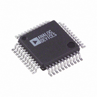
AD7865BS-1 Analog Devices Inc, AD7865BS-1 Datasheet - Page 7

AD7865BS-1
Manufacturer Part Number
AD7865BS-1
Description
IC ADC 14BIT 4CH 5V 44-MQFP
Manufacturer
Analog Devices Inc
Specifications of AD7865BS-1
Rohs Status
RoHS non-compliant
Number Of Bits
14
Sampling Rate (per Second)
350k
Data Interface
Parallel
Number Of Converters
1
Power Dissipation (max)
160mW
Voltage Supply Source
Analog and Digital
Operating Temperature
-40°C ~ 85°C
Mounting Type
Surface Mount
Package / Case
44-MQFP, 44-PQFP
Available stocks
Company
Part Number
Manufacturer
Quantity
Price
Company:
Part Number:
AD7865BS-1
Manufacturer:
ADI
Quantity:
329
Pin
24
25
26
27–34
35
36
37
38, 39
40–43
44
Mnemonic
V
AV
AGND
DB13–DB6
DV
V
DGND
DB5, DB4
DB3–DB0
EOC
REF
DRIVE
DD
DD
Description
Reference Input/Output. This pin provides access to the internal reference (2.5 V ± 20 mV)
and also allows the internal reference to be overdriven by an external reference source (2.5 V
± 5%). A 0.1 µF decoupling capacitor should be connected between this pin and AGND.
Analog Positive Supply Voltage, 5.0 V ± 5%. A 0.1 µF decoupling capacitor should be con-
nected between this pin and AGND.
Analog Ground. General Analog Ground. This AGND pin should be connected to the system’s
AGND plane.
Data Bit 13 is the MSB, followed by Data Bit 12 to Data Bit 6. Three-state TTL outputs.
Output coding is twos complement for AD7865-1 and AD7865-3, and straight binary for
AD7865-2.
Positive Supply Voltage for Digital section, 5.0 V ± 5%. A 0.1 µF decoupling capacitor should
be connected between this pin and AGND. Both DV
together.
This pin provides the positive supply voltage for the output drivers (DB0 to DB13), BUSY,
EOC and FRSTDATA. It is normally tied to DV
0.1 µF capacitor. It allows improved performance when reading during the conversion
sequence. Also, the output data drivers may be powered by a 3 V ± 10% supply to facilitate
interfacing to 3 V processors and DSPs.
Digital Ground. Ground reference for Digital circuitry. This DGND pin should be connected
to the system’s DGND plane. The system’s DGND and AGND planes should be connected
together at one point only, preferably at an AGND pin.
Data Bit 5 to Data Bit 4. Three-state TTL outputs.
Data Bit 3 to Data Bit 0. Bidirectional data pins. When a read operation takes place, these
pins are three-state TTL outputs. The channel select register is programmed with the data on
the DB0–DB3 pins with standard CS and WR signals. DB0 represents Channel 1 and DB3
represents Channel 4.
End-of-Conversion. Active low logic output indicating conversion status. The end of each
conversion in a conversion sequence is indicated by a low going pulse on this line.
DD
. V
DD
DRIVE
and AV
should be decoupled with a
DD
should be externally tied
AD7865


