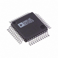
AD7865BS-3 Analog Devices Inc, AD7865BS-3 Datasheet - Page 17

AD7865BS-3
Manufacturer Part Number
AD7865BS-3
Description
IC ADC 14BIT 4CH 5V 44-MQFP
Manufacturer
Analog Devices Inc
Specifications of AD7865BS-3
Rohs Status
RoHS non-compliant
Number Of Bits
14
Sampling Rate (per Second)
350k
Data Interface
Parallel
Number Of Converters
1
Power Dissipation (max)
160mW
Voltage Supply Source
Analog and Digital
Operating Temperature
-40°C ~ 85°C
Mounting Type
Surface Mount
Package / Case
44-MQFP, 44-PQFP
AC Linearity Plots
The plots shown in Figure 18 below show typical DNL and INL
for the AD7865.
MICROPROCESSOR INTERFACING
The high speed parallel interface of the AD7865 allows easy
interfacing to most DSPs and microprocessors. The AD7865
interface of the AD7865 consists of the data lines (DB0 to
DB13), CS, RD, WR, EOC and BUSY.
AD7865–ADSP-21xx Interface
Figure 19 shows an interface between the AD7865 and the
ADSP-210x. The CONVST signal can be generated by the
ADSP-210x or from some other external source. Figure 19
shows the CS being generated by a combination of the DMS
signal and the address bus of the ADSP-2100. In this way the
AD7865 is mapped into the data memory space of the
ADSP-210x.
The AD7865 BUSY line provides an interrupt to the ADSP-
210x when the conversion sequence is complete on all the
selected channels. The conversion results can then be read from
the AD7865 using successive read operations. Alternately, one
can use the EOC pulse to interrupt the ADSP-210x when the
conversion on each channel is complete when reading between
each conversion in the conversion sequence (Figure 8). The
AD7865 is read using the following instruction
where MR0 is the ADSP-210x MR0 register and ADC is the
AD7865 address.
–0.60
–0.60
0.60
0.60
0
0
0
0
4000
4000
MR0 = DM(ADC)
ADC – Code
ADC – Code
8000
8000
12000
12000
16383
16383
AD7865–TMS320C5x Interface
Figure 20 shows an interface between the AD7865 and the
TMS320C5x. As with the previous interfaces, conversion can be
initiated from the TMS320C5x or from an external source and
the processor is interrupted when the conversion sequence is
completed. The CS signal to the AD7865 derived from the DS
signal and a decode of the address bus. This maps the AD7865
into external data memory. The RD signal from the TMS320 is
used to enable the ADC data onto the data bus. The AD7865
has a fast parallel bus so there are no wait state requirements.
The following instruction is used to read the conversion results
from the AD7865:
where D is Data Memory address and ADC is the AD7865
address.
AD7865–MC68000 Interface
An interface between the AD7865 and the MC68000 is shown
in Figure 21. The conversion can be initiated from the MC68000
or from an external source. The AD7865 BUSY line can be
used to interrupt the processor or, alternatively, software delays
can ensure that conversion has been completed before a read to
the AD7865 is attempted. Because of the nature of its inter-
rupts, the 68000 requires additional logic (not shown in Figure
21) to allow it to be interrupted correctly. For further informa-
tion on 68000 interrupts, consult the 68000 users manual.
V
V
V
V
V
V
V
V
IN1
IN2
IN3
IN4
IN1
IN2
IN3
IN4
AD7865
AD7865
DB0–DB13
DB0–DB13
CONVST
CONVST
BUSY
BUSY
WR
WR
RD
CS
CS
RD
IN D,ADC
ADDRESS
ADDRESS
DECODE
DECODE
A0–A13
DMS
RD
WR
D0–D13
IRQn
DT1/F0
PA0
A0–A13
DS
RD
WR
D0–D13
INTn
TMS320C5x
ADSP-21xx
AD7865


