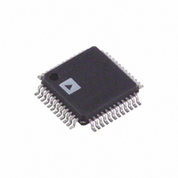
AD9288BST-80 Analog Devices Inc, AD9288BST-80 Datasheet

AD9288BST-80
Specifications of AD9288BST-80
Available stocks
Related parts for AD9288BST-80
AD9288BST-80 Summary of contents
Page 1
FEATURES Dual 8-bit, 40 MSPS, 80 MSPS, and 100 MSPS ADC Low power 100 MSPS per channel On-chip reference and track-and-hold 475 MHz analog bandwidth each channel SNR = MHz 1 V p-p ...
Page 2
AD9288 TABLE OF CONTENTS Specifications..................................................................................... 3 Explanation of Test Levels ........................................................... 4 Timing Diagrams.......................................................................... 5 Absolute Maximum Ratings............................................................ 7 ESD Caution.................................................................................. 7 Pin Configuration and Function Descriptions............................. 8 Typical Performance Characteristics ............................................. 9 Test Circuits..................................................................................... 12 Terminology .................................................................................... 13 Theory ...
Page 3
... VI Logic 0 Voltage Full VI POWER SUPPLY 4 Power Dissipation Full Standby Dissipation Full VI 25°C I Power Supply Rejection Ratio (PSRR) AD9288BST-100 AD9288BST-80 Min Typ Max Min Typ 8 8 ± 0.5 +1.25 ± 0.5 1.50 ± 0.50 +1.25 ± 0.50 1.50 Guaranteed Guaranteed –6 ± ...
Page 4
... II 100% production tested at 25 III Sample tested only. IV Parameter is guaranteed by design and characterization testing. V Parameter is a typical value only. VI 100% production tested at 25 100% production tested at temperature extremes for military devices. AD9288BST-100 AD9288BST-80 Min Typ Max Min Typ 47.5 47.5 47.5 ...
Page 5
TIMING DIAGRAMS SAMPLE ENCODE –D0 DATA N – –D0 DATA N – Figure 2. Normal Operation, Same Clock (S1 ...
Page 6
AD9288 SAMPLE SAMPLE ENCODE A ENCODE B D7 – DATA N – – DATA N – 9 Figure 4. Data ...
Page 7
ABSOLUTE MAXIMUM RATINGS Table 2. Parameter Analog Inputs Digital Inputs VREF IN Digital Output Current Operating Temperature Storage Temperature Maximum Junction Temperature Maximum Case Temperature Thermal Impedance θ ja ESD CAUTION ESD (electrostatic discharge) sensitive ...
Page 8
AD9288 PIN CONFIGURATION AND FUNCTION DESCRIPTIONS Table 3. Pin No. Name Description 1, 12, 16, 27, 29, GND Ground 32, 34 Analog Input for Channel Analog Input for Channel A (Complementary). ...
Page 9
TYPICAL PERFORMANCE CHARACTERISTICS 0 ENCODE = 100MSPS A = 10.3MHz IN –10 SNR = 48.52dB SINAD = 48.08dB –20 SECOND HARMONIC = –62.54dBc THIRD HARMONIC = –63.56dBc –30 –40 –50 –60 –70 –80 –90 SAMPLE Figure 6. Spectrum ...
Page 10
AD9288 10.3MHz IN SNR SINAD MSPS Figure 12. SINAD/SNR vs. Encode Rate 50 SNR SINAD 7.0 6.5 6.0 5.5 5.0 4.5 ENCODE ...
Page 11
CODE Figure 18. Integral Nonlinearity 1.00 0.75 0.50 0.25 0 –0.25 –0.50 –0.75 –1.00 CODE Figure 19. Differential Nonlinearity 1.3 1.2 1.1 1.0 0.9 0.8 0.7 0 0.25 0.50 Figure 20. ...
Page 12
AD9288 TEST CIRCUITS V D 28kΩ 12kΩ Figure 21. Equivalent Analog Input Circuit BIAS REF IN Figure 22. Equivalent Reference Input Circuit ENCODE Figure 23. Equivalent Encode Input Circuit 28kΩ 12kΩ ...
Page 13
TERMINOLOGY Analog Bandwidth (Small Signal) The analog input frequency at which the spectral power of the fundamental frequency (as determined by the FFT analysis) is reduced by 3 dB. Aperture Delay The delay between a 50% crossing of Encode and ...
Page 14
AD9288 THEORY OF OPERATION The AD9288 ADC architecture is a bit-per-stage pipeline-type converter utilizing switch capacitor techniques. These stages determine the 5 MSBs and drive a 3-bit flash. Each stage provides sufficient overlap and error correction, allowing optimization of comparator ...
Page 15
AD9218/AD9288 CUSTOMER PCB BOM Table 5. Bill of Materials No. Qty. Reference Designator 1 29 C1, C3-C15, C20, C21, C24, C25, C27, C30–C35, C39–C42 2 2 C2, C36 3 7 C16–C19, C26, C37, C38 4 28 E1, E2, E3, E4, ...
Page 16
AD9288 EVALUATION BOARD The AD9218/AD9288 customer evaluation board offers an easy way to test the AD9218 or the AD9288. The compatible pinout of the two parts facilitates the use of one PCB for testing either part. The PCB requires power ...
Page 17
(MSB ...
Page 18
AD9288 Figure 27. PCB Schematic (Continued) Rev Page 00585-027 ...
Page 19
Figure 28. Top Silkscreen Figure 29. Top Routing Figure 30. Ground Plane Rev Page AD9288 Figure 31. Split Power Plane Figure 32. Bottom Routing Figure 33. Bottom Silkscreen ...
Page 20
AD9288 TROUBLESHOOTING If the board does not seem to be working correctly, try the following: • Verify power at the IC pins. • Check that all jumpers are in the correct position for the desired mode of operation. • Verify ...
Page 21
... Model Temperature Range –40°C to +85°C AD9288BST-40 1 AD9288BSTZ-40 –40°C to +85°C 1 –40°C to +85°C AD9288BSTZRL-40 –40°C to +85°C AD9288BST-80 1 AD9288BSTZ-80 –40°C to +85°C –40°C to +85°C AD9288BST-100 1 AD9288BSTZ-100 –40°C to +85°C AD9288/PCB Pb-free part. ...
Page 22
AD9288 NOTES Rev Page ...
Page 23
NOTES Rev Page AD9288 ...
Page 24
AD9288 NOTES © 2004 Analog Devices, Inc. All rights reserved. Trademarks and registered trademarks are the property of their respective owners. C00585–0–12/04(C) Rev Page ...


