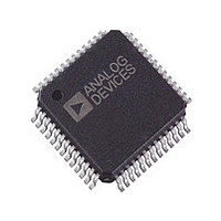
AD9432BST-105 Analog Devices Inc, AD9432BST-105 Datasheet

AD9432BST-105
Specifications of AD9432BST-105
Available stocks
Related parts for AD9432BST-105
AD9432BST-105 Summary of contents
Page 1
FEATURES On-chip reference and track-and-hold On-chip input buffer Power dissipation: 850 mW typical at 105 MSPS 500 MHz analog bandwidth SNR MHz AIN at 105 MSPS SFDR MHz AIN at 105 MSPS ...
Page 2
AD9432 TABLE OF CONTENTS Features .............................................................................................. 1 Applications ....................................................................................... 1 General Introduction ....................................................................... 1 Functional Block Diagram .............................................................. 1 Revision History ............................................................................... 2 Specifications ..................................................................................... 3 Timing Diagram ........................................................................... 5 Absolute Maximum Ratings ............................................................ 6 Explanation of Test Levels ........................................................... ...
Page 3
SPECIFICATIONS 5.0 V; external reference; differential encode input, unless otherwise noted Table 1. Parameter Temp RESOLUTION DC ACCURACY Differential Nonlinearity (DNL) 25°C Full Integral Nonlinearity (INL) 25°C Full No Missing Codes Full ...
Page 4
AD9432 Parameter Temp POWER SUPPLY 3 Power Dissipation Full I Full VCC I Full VDD Power Supply Rejection Ratio 25°C (PSRR) 4 DYNAMIC PERFORMANCE Signal-to-Noise Ratio (SNR) (Without Harmonics MHz 25° MHz 25°C ...
Page 5
TIMING DIAGRAM SAMPLE N SAMPLE N – 1 AIN ENCODE ENCODE D11 TO D0 DATA N – SAMPLE SAMPLE DATA DATA DATA N – 10 DATA N ...
Page 6
AD9432 ABSOLUTE MAXIMUM RATINGS Table 2. Parameter Analog Inputs Digital Inputs VREFIN Digital Output Current Operating Temperature Range Storage Temperature Range Maximum Junction Temperature Maximum Case Temperature Stresses above those listed under Absolute Maximum Ratings may ...
Page 7
PIN CONFIGURATIONS AND FUNCTION DESCRIPTIONS GND 1 PIN GND 3 GND AD9432 TOP VIEW CC (Not to ...
Page 8
AD9432 TYPICAL PERFORMANCE CHARACTERISTICS 100 ENCODE (MSPS) Figure 5. SNR/SINAD/SFDR vs –50 –55 –60 –65 –70 –75 –80 –85 3RD –90 2ND –95 –100 0 20 ...
Page 9
ENCODE = 105MSPS –10 AIN = 10.3MHz (–0.53dBFS) SNR = 67.32dB –20 SINAD = 67.07dB –30 SFDR = –85dBc –40 –50 –60 –70 –80 –90 –100 –110 –120 FREQUENCY Figure 11. FFT 105 MSPS 10.3 ...
Page 10
AD9432 110 100 dBFS 90 80 ENCODE = 105MSPS 70 AIN = 50.3MHz 60 50 dBc –80 –70 –60 –50 –40 –30 ANALOG INPUT POWER LEVEL (dBFS) Figure 17. Single-Tone SFDR 105 MSPS, ...
Page 11
TERMINOLOGY Analog Bandwidth The analog input frequency at which the spectral power of the fundamental frequency (as determined by the FFT analysis) is reduced by 3 dB. Aperture Delay The delay between a differential crossing of ENCODE and ENCODE and ...
Page 12
AD9432 EQUIVALENT CIRCUITS V CC VREFIN Figure 21. Voltage Reference Input Circuit V CC VREFOUT Figure 22. Voltage Reference Output Circuit V CC 17kΩ ENCODE 100Ω 8kΩ Figure 23. Encode Input Circuit 17kΩ ENCODE 100Ω 8kΩ Rev Page ...
Page 13
THEORY OF OPERATION The AD9432 is a 12-bit pipeline converter that uses a switched- capacitor architecture. Optimized for high speed, this converter provides flat dynamic performance up to frequencies near Nyquist. DNL transitional errors are calibrated at final test to ...
Page 14
AD9432 DIGITAL OUTPUTS The digital outputs are 3 3.6 V) TTL-/CMOS- compatible for lower power consumption. The output data format is twos complement (see Table 6). Table 6. Twos Complement Output Coding (V AIN − AIN ...
Page 15
APPLICATIONS INFORMATION USING THE AD8138 TO DRIVE THE AD9432 The AD8138 differential output op amp can be used to drive the AD9432 in dc-coupled applications. The AD8138 was specifically designed for ADC driver applications. Superior SNR performance is maintained up ...
Page 16
... COPLANARITY VIEW A ROTATED 90 ° CCW ORDERING GUIDE Model Temperature Range 1 AD9432BSTZ-80 −40°C to +85°C 1 AD9432BSTZ-105 −40°C to +85°C 1 AD9432BSVZ-80 −40°C to +85°C AD9432BSVZ-105 1 −40°C to +85° RoHS Compliant Part. ©2002–2009 Analog Devices, Inc. All rights reserved. Trademarks and registered trademarks are the property of their respective owners ...


