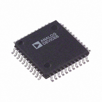
AD2S1200WSTZ Analog Devices Inc, AD2S1200WSTZ Datasheet - Page 16

AD2S1200WSTZ
Manufacturer Part Number
AD2S1200WSTZ
Description
IC R/D CONV W/REF OSCIL 44-LQFP
Manufacturer
Analog Devices Inc
Type
R/D Converterr
Datasheet
1.AD2S1200.pdf
(24 pages)
Specifications of AD2S1200WSTZ
Resolution (bits)
12 b
Data Interface
Serial, Parallel
Voltage Supply Source
Analog and Digital
Voltage - Supply
4.75 V ~ 5.25 V
Operating Temperature
-40°C ~ 125°C
Mounting Type
Surface Mount
Package / Case
44-LQFP
Input Channel Type
Differential
Supply Voltage Range - Analog
4.75V To 5.25V
Supply Voltage Range - Digital
4.75V To 5.25V
Lead Free Status / RoHS Status
Lead free / RoHS Compliant
For Use With
EVAL-AD2S1200CBZ - BOARD EVAL FOR AD2S1200
Sampling Rate (per Second)
-
Lead Free Status / RoHS Status
Lead free / RoHS Compliant, Lead free / RoHS Compliant
Available stocks
Company
Part Number
Manufacturer
Quantity
Price
Company:
Part Number:
AD2S1200WSTZ
Manufacturer:
Analog Devices Inc
Quantity:
135
Company:
Part Number:
AD2S1200WSTZ
Manufacturer:
ADI
Quantity:
276
Company:
Part Number:
AD2S1200WSTZ
Manufacturer:
Analog Devices Inc
Quantity:
10 000
AD2S1200
INCREMENTAL ENCODER OUTPUTS
The incremental encoder emulation outputs A, B, and NM are
free running and are always valid, providing that valid resolver
format input signals are applied to the converter.
The AD2S1200 emulates a 1024-line encoder. Relating this to
converter resolution means one revolution produces 1,024 A, B
pulses. A leads B for increasing angular rotation (i.e., clockwise
direction). The addition of the DIR output negates the need for
external A and B direction decode logic. The DIR output
indicates the direction of the input rotation and it is high for
increasing angular rotation. DIR can be considered as an
asynchronous output and can make multiple changes in state
between two consecutive LSB update cycles. This occurs when
the direction of rotation of the input changes but the magnitude
of the rotation is less than 1 LSB.
The north marker pulse is generated as the absolute angular
position passes through zero. The north marker pulse width is
set internally for 90° and is defined relative to the A cycle.
Figure 9 details the relationship between A, B, and NM.
Unlike incremental encoders, the AD2S1200 encoder output is
not subject to error specifications such as cycle error, eccentric-
ity, pulse and state width errors, count density, and phase ϕ. The
maximum speed rating, n , of an encoder is calculated from its
maximum switching frequency, f
lution ( PPR ).
The AD2S1200 A, B pulses are initiated from XTALOUT, which
has a frequency of 4.096 MHz. The equivalent encoder
switching frequency is
NM
A
B
1
4 /
Figure 9. A, B, and NM Timing for Clockwise Rotation
×
. 4
096
MHz
=
n
. 1
=
024
60
MHz
×
PPR
MAX
f
MAX
, and its pulses per revo-
4 (
Updates
=
1
Pulse
)
Rev. 0 | Page 16 of 24
At 12 bits, the PPR = 1,024. Therefore, the maximum speed, n,
of the AD2S1200 is
To get a maximum speed of 60,000 rpm, an external crystal of
8.192 MHz has to be chosen in order to produce an internal
CLOCKOUT equal to 4.096 MHz.
This compares favorably with encoder specifications where f
is specified from 20 kHz (photo diodes) to 125 kHz (laser
based) depending on the light system used. A 1,024 line laser-
based encoder will have a maximum speed of 7,300 rpm.
The inclusion of A, B outputs allows the AD2S1200 plus
resolver solution to replace optical encoders directly without the
need to change or upgrade existing application software.
ON-BOARD PROGRAMMABLE SINUSOIDAL
OSCILLATOR
An on-board oscillator provides the sinusoidal excitation signal
(EXC) to the resolver as well as its complemented signal ( EXC ).
The frequency of this reference signal is programmable to four
standard frequencies (10 kHz, 12 kHz, 15 kHz, or 20 kHz) using
the FS1 and FS2 pins (see Table 7). FS1 and FS2 have internal pull-
ups, so the default frequency is 10 kHz. The amplitude of this
signal is centered on 2.5 V and has an amplitude of 3.6 V p-p.
Table 7. Excitation Frequency Selection
Frequency Selection (kHz)
10
12
15
20
The reference output of the AD2S1200 will need an external
buffer amplifier to provide gain and the additional current to
drive a resolver. Refer to Figure 6 for a suggested buffer circuit.
The AD2S1200 also provides an internal synchronous reference
signal that is phase locked to its Sin and Cos inputs. Phase
errors between the resolver primary and secondary windings
could degrade the accuracy of the RDC and are compensated by
this synchronous reference signal. This also compensates the
phase shifts due to temperature and cabling and eliminates the
need of an external preset phase compensation circuits.
n
=
60
×
, 1
, 1
024
024
,
000
FS1
1
1
0
0
=
60000
rpm
FS2
1
0
1
0
MAX


