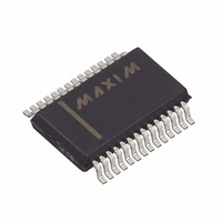
MAX1270BCAI+ Maxim Integrated Products, MAX1270BCAI+ Datasheet - Page 17

MAX1270BCAI+
Manufacturer Part Number
MAX1270BCAI+
Description
IC ADC 12-BIT MULTIRANGE 28-SSOP
Manufacturer
Maxim Integrated Products
Type
Data Acquisition System (DAS), ADCr
Datasheet
1.MAX1270BCAI.pdf
(20 pages)
Specifications of MAX1270BCAI+
Resolution (bits)
12 b
Sampling Rate (per Second)
110k
Data Interface
Serial
Voltage Supply Source
Single Supply
Voltage - Supply
4.75 V ~ 5.25 V
Operating Temperature
0°C ~ 70°C
Mounting Type
Surface Mount
Package / Case
28-SSOP
Number Of Adc Inputs
8
Architecture
SAR
Conversion Rate
110 KSPs
Resolution
12 bit
Interface Type
3-Wire (SPI, QSPI, MICROWIRE)
Voltage Reference
Internal 4.096 V or External
Supply Voltage (max)
5 V
Maximum Power Dissipation
762 mW
Maximum Operating Temperature
+ 85 C
Mounting Style
SMD/SMT
Minimum Operating Temperature
- 40 C
Lead Free Status / RoHS Status
Lead free / RoHS Compliant
ry in unipolar mode with 1 LSB = (FS / 4096) and two’s
complement binary in bipolar mode with 1 LSB = [(2 x
Output data coding for the MAX1270/MAX1271 is bina-
| FS | ) / 4096]. Code transitions occur halfway between
successive-integer LSB values. Figures 14a and 14b
show the input/output (I/O) transfer functions for unipo-
lar and bipolar operations, respectively. For full-scale
values, refer to Table 3.
Careful PC board layout is essential for best system
performance. Use a ground plane for best perfor-
mance. To reduce crosstalk and noise injection, keep
analog and digital signals separate. Connect analog
grounds and DGND in a star configuration to AGND.
For noise-free operation, ensure the ground return from
AGND to the supply ground is low impedance and as
short as possible. Connect the logic grounds directly to
the supply ground. Bypass V
capacitors to AGND to minimize highand low-frequency
fluctuations. If the supply is excessively noisy, connect
a 5Ω resistor between the supply and V
Figure 15.
Figure 14a. Unipolar Transfer Function
00... 011
00... 010
00... 001
00... 000
11... 111
11... 110
11... 101
OUTPUT CODE
0
1
2
Layout, Grounding, and Bypassing
______________________________________________________________________________________
3
INPUT VOLTAGE (LSB)
FULL-SCALE
TRANSITION
DD
Transfer Function
with 0.1µF and 4.7µF
FS -
DD
3
/
, as shown in
2
LSB
1 LSB =
FS
Multirange, +5V, 8-Channel,
4096
FS
Figure 14b. Bipolar Transfer Function
Figure 15. Power-Supply Grounding Connections
011... 111
011... 110
000... 001
000... 000
111... 111
100... 010
100... 001
100... 000
*OPTIONAL
**CONNECT AGND AND DGND WITH A GROUND PLANE OR A SHORT TRACE.
R* = 5Ω
OUTPUT CODE
+5V
V
DD
Serial 12-Bit ADCs
-FS
0.1µF
4.7µF
AGND
MAX1270
MAX1271
INPUT VOLTAGE (LSB)
**
SUPPLY
0
DGND
+FS - 1 LSB
+5V
CIRCUITRY
DIGITAL
1 LSB =
GND
DGND
2|FS|
4096
17


