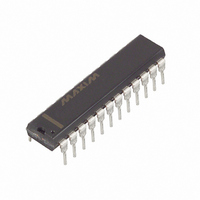
MAX1270ACNG+ Maxim Integrated Products, MAX1270ACNG+ Datasheet - Page 11

MAX1270ACNG+
Manufacturer Part Number
MAX1270ACNG+
Description
IC ADC 12BIT MULTIRANGE 24-DIP
Manufacturer
Maxim Integrated Products
Type
Data Acquisition System (DAS), ADCr
Datasheet
1.MAX1270BCAI.pdf
(20 pages)
Specifications of MAX1270ACNG+
Resolution (bits)
12 b
Sampling Rate (per Second)
100k
Data Interface
Serial
Voltage Supply Source
Single Supply
Voltage - Supply
4.75 V ~ 5.25 V
Operating Temperature
0°C ~ 70°C
Mounting Type
Through Hole
Package / Case
24-DIP (0.300", 7.62mm)
Number Of Adc Inputs
8
Architecture
SAR
Conversion Rate
110 KSPs
Resolution
12 bit
Input Type
Voltage
Interface Type
3-Wire (SPI, QSPI, MICROWIRE)
Voltage Reference
Internal 4.096 V or External
Supply Voltage (max)
5 V
Maximum Power Dissipation
1067 mW
Maximum Operating Temperature
+ 70 C
Mounting Style
Through Hole
Minimum Operating Temperature
0 C
Lead Free Status / RoHS Status
Lead free / RoHS Compliant
Table 1. Control-Byte Format
Table 2. Channel Selection
Table 3. Range and Polarity Selection for MAX1270/MAX1271
RANGE AND POLARITY SELECTION FOR THE MAX1270
RANGE AND POLARITY SELECTION FOR THE MAX1271
1, 0 (LSB)
7 (MSB)
SEL2
START
(MSB)
6, 5, 4
INPUT RANGE
INPUT RANGE
BIT 7
BIT
0
0
0
0
1
1
1
1
0 to V
3
2
0 to +10V
0 to V
0 to +5V
±V
±V
±10V
±5V
REF
REF
REF
REF
/2
/2
SEL2, SEL1,
SEL1
PD1, PD0
0
0
1
1
0
0
1
1
START
NAME
______________________________________________________________________________________
BIT 6
SEL2
SEL0
RNG
BIP
RNG
RNG
0
1
0
1
0
1
0
1
SEL0
First logic 1 after CS goes low defines the beginning of the control byte.
These 3 bits select the desired “on” channel (Table 2).
Selects the full-scale input voltage range (Table 3).
Selects the unipolar or bipolar conversion mode (Table 3).
Select clock and power-down modes (Table 4).
0
1
0
1
0
1
0
1
BIT 5
SEL1
BIP
BIP
0
0
1
1
0
0
1
1
CHANNEL
CH0
CH1
CH2
CH3
CH4
CH5
CH6
CH7
-V
-V
FULL SCALE
FULL SCALE
BIT 4
SEL0
REF
REF
Negative
Negative
-V
-V
Multirange, +5V, 8-Channel,
REF
—
—
x 1.2207
x 2.4414
—
—
REF
/2
BIT 3
RNG
Table 4. Power-Down and Clock Selection
PD1
0
0
1
1
DESCRIPTION
PD0
SCALE (V)
SCALE (V)
0
1
0
1
ZERO
ZERO
Serial 12-Bit ADCs
BIT 2
0
0
0
0
0
0
0
0
BIP
Normal operation (always on), internal clock
mode.
Normal operation (always on), external clock
mode.
Standby power-down mode (STBYPD), clock
mode unaffected.
Full power-down mode (FULLPD), clock mode
unaffected.
BIT 1
PD1
MODE
FULL SCALE
V
V
V
V
FULL SCALE
REF
REF
REF
REF
V
V
V
V
REF
REF
x 1.2207
x 2.4414
x 1.2207
x 2.4414
REF
REF
/2
/2
(LSB)
BIT 0
PD0
11


