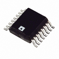
AD7843ARQZ Analog Devices Inc, AD7843ARQZ Datasheet - Page 17

AD7843ARQZ
Manufacturer Part Number
AD7843ARQZ
Description
IC ADC 12BIT TOUCHSCREEN 16-QSOP
Manufacturer
Analog Devices Inc
Type
Resistiver
Datasheet
1.AD7843ARUZ.pdf
(20 pages)
Specifications of AD7843ARQZ
Resolution (bits)
12 b
Data Interface
Serial
Touch Panel Interface
4-Wire
Number Of Inputs/keys
1 TSC
Data Rate/sampling Rate (sps, Bps)
125k
Voltage Reference
External
Voltage - Supply
2.2 V ~ 5.25 V
Operating Temperature
-40°C ~ 85°C
Mounting Type
Surface Mount
Package / Case
16-QSOP
Voltage Supply Source
Single Supply
Sampling Rate (per Second)
125k
Sampling Rate
125kSPS
Supply Current
240µA
Digital Ic Case Style
QSOP
No. Of Pins
16
Operating Temperature Range
-40°C To +85°C
Lead Free Status / RoHS Status
Lead free / RoHS Compliant
For Use With
EVAL-AD7843EBZ - BOARD EVAL FOR AD7843
Lead Free Status / RoHS Status
Lead free / RoHS Compliant, Lead free / RoHS Compliant
Available stocks
Company
Part Number
Manufacturer
Quantity
Price
Company:
Part Number:
AD7843ARQZ
Manufacturer:
ADI
Quantity:
196
Part Number:
AD7843ARQZ
Manufacturer:
ADI/亚德诺
Quantity:
20 000
DETAILED SERIAL INTERFACE TIMING
Figure 25 shows the detailed timing diagram for serial
interfacing to the AD7843. Writing information to the control
register takes place on the first eight rising edges of DCLK in a
data transfer. The control register is written to only if a START
bit is detected (see the Control Register section) on DIN. The
initiation of the following conversion also depends on the
presence of the START bit. Throughout the eight DCLK cycles
when data is being written to the part, the DOUT line is driven
low. The MSB of the conversion result is clocked out on the
falling edge of the ninth DCLK cycle and is valid on the rising
edge of the tenth DCLK cycle; therefore, nine leading zeros can
be clocked out prior to the MSB. This means the data seen on
the DOUT line in the 24 DCLK conversion cycle is presented in
the form of nine leading zeros, twelve bits of data, and three
trailing zeros.
The rising edge of CS puts the bus and the BUSY output back
into three-state, the DIN line is ignored, and, if a conversion is
in progress at the time, this is also aborted. However, if CS is not
brought high after the completion of the conversion cycle, then
DOUT
DCLK
BUSY
DIN
CS
t
t
1
3
t
2
t
7
t
t
8
4
t
5
Figure 25. Detailed Timing Diagram
PD0
t
6
Rev. B | Page 17 of 20
DB11
t
6
the part waits for the next START bit to initiate the next
conversion. This means that each conversion does not
necessarily need to be framed by CS , because once CS goes low,
the part detects each START bit and clocks in the control word
after it on DIN. When the AD7843 is in the 12-bit conversion
mode, a second START bit is not detected until seven DCLK
pulses have elapsed after a control word is clocked in on DIN,
that is, another START bit can be clocked in on the eighth
DCLK rising edge after a control word is written to the device
(see the Fifteen Clocks per Cycle section). If the device is in the
8-bit conversion mode, a second START bit is not recognized
until three DCLK pulses elapse after the control word is clocked
in, that is, another START bit can be clocked in on the fourth
DCLK rising edge after a control word is written to the device.
Because a START bit can be recognized during a conversion, the
control word for the next conversion can be clocked in during
the current conversion, enabling the AD7843 to complete a
conversion cycle in less than 24 DCLKs.
t
DB10
9
t
11
t
10
t
12
AD7843


