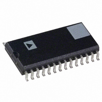
ADV7128KR80 Analog Devices Inc, ADV7128KR80 Datasheet - Page 6

ADV7128KR80
Manufacturer Part Number
ADV7128KR80
Description
IC DAC VIDEO 80MHZ 5.0V 28SOIC
Manufacturer
Analog Devices Inc
Type
Video DACr
Datasheet
1.ADV7128KR30.pdf
(8 pages)
Specifications of ADV7128KR80
Rohs Status
RoHS non-compliant
Resolution (bits)
10 b
Sampling Rate (per Second)
80M
Voltage Supply Source
Single Supply
Voltage - Supply
4.75 V ~ 5.25 V
Operating Temperature
0°C ~ 70°C
Mounting Type
Surface Mount
Package / Case
28-SOIC (7.5mm Width)
Data Interface
-
Available stocks
Company
Part Number
Manufacturer
Quantity
Price
ADV7128
Reference Input
An external 1.23 V voltage reference is required to drive the
ADV7128. The AD589 from Analog Devices is an ideal choice
of reference. It is a two-terminal, low cost, temperature com-
pensated bandgap voltage reference which provides a fixed
1.23 V output voltage for input currents between 50 A and
5 mA. Figure 4 shows a typical reference circuit connection dia-
gram. The voltage reference gets its current drive from the
ADV7128’s V
pin. A 0.1 F ceramic capacitor is required between the COMP
pin and V
the internal reference amplifier.
A resistance R
mines the amplitude of the output video level according to the
following equation:
Using a variable value of R
accurate adjustment of the analog output video levels. Use of a
fixed 560
quoted in the specification page. These values typically corre-
spond to the RS-343A video waveform values as shown in
Figure 3.
D/A Converter
The ADV7128 contains a 10-bit D/A converter. The DAC is
designed using an advanced, high speed, segmented architec-
ture. The bit currents corresponding to each digital input are
routed to either the analog output (bit = “1”) or GND (bit =
“0”) by a sophisticated decoding scheme. The use of identical
current sources in a monolithic design guarantees monotonicity
and low glitch. The on-board operational amplifier stabilizes the
full-scale output current against temperature and power supply
variations.
Analog Output
The analog output of the ADV7128 is a high impedance current
source. The current output is capable of directly driving a
37.5
Figure 5a shows the required configuration for the output con-
nected into a doubly terminated 75
*ADDITIONAL CIRCUITRY, INCLUDING DECOUPLING COMPONENTS,
EXCLUDED FOR CLARITY
I
OUT
TO DAC
COMP
(mA) = 7,969
load, such as a doubly terminated 75
AA
ADV7128
. This is necessary so as to provide compensation for
R
SET
AA
SET
ANALOG POWER PLANE
0.01 F
through an on-board 1 k resistor to the V
Figure 4. Reference Circuit
resistor yields the analog output levels as
connected between R
1k
V
REF
SET
(V)/R
V
V
GND
RSET
AA
REF
, as shown in Figure 4, allows for
560
R
SET
SET
+
5V
( )
I
load. This arrangement
REF
500
100
SET
~ ~
5mA
and GND deter-
coaxial cable.
AD589
(1.235V
VOLTAGE
REFERENCE)
REF
(1)
–6–
will develop RS-343A video output voltage levels across a 75
monitor.
A suggested method of driving RS-170 video levels into a 75
monitor is shown in Figure 5b. The output current level of the
DAC remains unchanged, but the source termination resistance,
Z
More detailed information regarding load terminations for vari-
ous output configurations, including RS-343A and RS-170, is
available in an Application Note entitled “Video Formats & Re-
quired Load Terminations” available from Analog Devices,
publication no. E1228-15-1/89.
Figure 3 shows the video waveforms associated with the current
output driving the doubly terminated 75
Gray Scale Operation
The ADV7128 can be used for stand-alone, gray scale (mono-
chrome) or composite video applications (i.e., only one channel
used for video information).
Video Output Buffer
The ADV7128 is specified to drive transmission line loads,
which is what most monitors are rated as. The analog output
configurations to drive such loads are described in the Analog
Interface section and illustrated in Figure 5. However, in some
applications it may be required to drive long “transmission line”
cable lengths. Cable lengths greater than 10 meters can attenu-
ate and distort high frequency analog output pulses. The inclu-
sion of output buffers will compensate for some cable distortion.
Buffers with large full power bandwidths and gains between 2
and 4 will be required. These buffers will also need to be able to
supply sufficient current over the complete output voltage
swing. Analog Devices produces a range of suitable op amps for
such applications. These include the AD84x series of monolithic
op amps. In very high frequency applications (80 MHz), the
AD9617 is recommended. More information on line driver buff-
ering circuits is given in the relevant op amp data sheets.
Use of buffer amplifiers also allows implementation of other
video standards besides RS-343A and RS-170. Altering the gain
components of the buffer circuit will result in any desired
video level.
S
, on the DAC is increased from 75
Figure 5a. Analog Output Termination for RS-343A
DAC
DAC
Figure 5b. Analog Output Termination for RS-170
TERMINATION)
TERMINATION)
Z
Z
S
(SOURCE
(SOURCE
S
= 75
= 150
I
I
OUT
OUT
Z
Z
(CABLE)
(CABLE)
O
O
= 75
= 75
to 150 .
load of Figure 5a.
(MONITOR)
Z
L
Z
(MONITOR)
L
= 75
= 75
REV. 0


