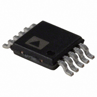
AD5290YRMZ10 Analog Devices Inc, AD5290YRMZ10 Datasheet - Page 6

AD5290YRMZ10
Manufacturer Part Number
AD5290YRMZ10
Description
IC DGTL POT 10K 256POS 10MSOP
Manufacturer
Analog Devices Inc
Datasheet
1.AD5290YRMZ50.pdf
(20 pages)
Specifications of AD5290YRMZ10
Taps
256
Resistance (ohms)
10K
Number Of Circuits
1
Temperature Coefficient
35 ppm/°C Typical
Memory Type
Volatile
Interface
SPI, 3-Wire Serial
Voltage - Supply
4.5 V ~ 30 V, ±4.5 V ~ 15 V
Operating Temperature
-40°C ~ 125°C
Mounting Type
Surface Mount
Package / Case
10-MSOP, Micro10™, 10-uMAX, 10-uSOP
Resistance In Ohms
10K
End To End Resistance
10kohm
No. Of Steps
256
Resistance Tolerance
± 30%
Supply Voltage Range
± 10V To ± 15V
Control Interface
Serial, SPI
No. Of Pots
Single
Lead Free Status / RoHS Status
Lead free / RoHS Compliant
For Use With
EVAL-AD5290EBZ - BOARD EVAL FOR AD5290
Lead Free Status / RoHS Status
Lead free / RoHS Compliant, Lead free / RoHS Compliant
Available stocks
Company
Part Number
Manufacturer
Quantity
Price
Company:
Part Number:
AD5290YRMZ10
Manufacturer:
ADI
Quantity:
453
Part Number:
AD5290YRMZ10
Manufacturer:
ADI/亚德诺
Quantity:
20 000
Part Number:
AD5290YRMZ10-R7
Manufacturer:
ADI/亚德诺
Quantity:
20 000
AD5290
Parameter
DYNAMIC CHARACTERISTICS
1
2
3
4
5
6
7
8
9
Typical represents average reading at +25°C, VDD = +15 V, and VSS = −15 V.
Resistor position nonlinearity error R-INL is the deviation from an ideal value measured between the maximum resistance and the minimum resistance wiper
positions. R-DNL measures the relative step change from an ideal value measured between successive tap positions. Parts are guaranteed monotonic.
All parts have a 35 ppm/°C temperature coefficient.
INL and DNL are measured at VW with the RDAC configured as a potentiometer divider similar to a voltage output DAC. VA = VDD and VB = 0 V. DNL specification
limits of ±1 LSB maximum are guaranteed monotonic operating conditions.
Resistor Terminal A, Terminal B, and Terminal W have no limitations on polarity with respect to each other.
Guaranteed by design and not subject to production test.
P
Bandwidth, noise, and settling times are dependent on the terminal resistance value chosen. The lowest R value results in the fastest settling time and highest
bandwidth. The highest R value results in the minimum overall power consumption.
All dynamic characteristics use VDD = +15 V and VSS = −15 V.
DISS
Bandwidth −3 dB
Total Harmonic Distortion
V
Resistor Noise Voltage
W
is calculated from (I
Settling Time
DD
× V
DD
) + abs (I
6, 8, 9
SS
× V
SS
). CMOS logic level inputs result in minimum power dissipation.
Symbol
THD
t
e
BW
S
N_WB
W
Rev. B | Page 6 of 20
Conditions
R
R
V
V
±1 LSB error band
R
AB
AB
A
A
WB
= 1 V rms, V
= 10 V, V
= 50 kΩ, code = 0x80
= 100 kΩ, code = 0x80
= 25 kΩ, f = 1 kHz
B
= 0 V,
B
= 0 V, f = 1 kHz
Min
Typ
90
50
0.002
4
20
1
Max
Unit
kHz
kHz
%
μs
nV√Hz


