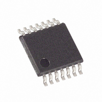
MAX5415EUD+ Maxim Integrated Products, MAX5415EUD+ Datasheet - Page 8

MAX5415EUD+
Manufacturer Part Number
MAX5415EUD+
Description
IC DGTL POT DUAL 256-TAP 14TSSOP
Manufacturer
Maxim Integrated Products
Datasheet
1.MAX5415EUD.pdf
(11 pages)
Specifications of MAX5415EUD+
Taps
256
Resistance (ohms)
100K
Number Of Circuits
2
Temperature Coefficient
35 ppm/°C Typical
Memory Type
Volatile
Interface
SPI, 3-Wire Serial
Voltage - Supply
2.7 V ~ 5.5 V
Operating Temperature
-40°C ~ 85°C
Mounting Type
Surface Mount
Package / Case
14-TSSOP
Resistance In Ohms
100K
Number Of Pots
Dual
Taps Per Pot
256
Resistance
100 KOhms
Wiper Memory
Volatile
Buffered Wiper
Non Buffered
Digital Interface
3-Wire (SPI)
Operating Supply Voltage
2.7 V to 5.5 V
Supply Current
0.8 uA
Maximum Operating Temperature
+ 85 C
Minimum Operating Temperature
- 40 C
Description/function
Dual 256-Tap, Low Drift, Digital Potentiometers in 14-TSSOP
Mounting Style
SMD/SMT
Supply Voltage (max)
5.5 V
Supply Voltage (min)
2.7 V
Tolerance
25 %
Lead Free Status / RoHS Status
Lead free / RoHS Compliant
have been shifted in, they are latched into the appropri-
ate potentiometer control register when CS transitions
from low to high. Note that if CS is not kept low during
the entire data stream, the data will be corrupted and
the device will need to be reloaded.
The first bit A0 (address bit) is used to address one or
the other of the potentiometers for programming.
Potentiometer control register A is selected for writing
when A0 is ‘zero,’ and potentiometer control register B
is selected when A0 is ‘one.’
The MAX5413/MAX5414/MAX5415 feature POR circuit-
ry that sets the wiper to the midscale position at power-
up.
The MAX5413/MAX5414/MAX5415 are intended for a
variety of circuits where accurate, fine-tuning adjustable
resistance is required, such as in adjustable voltage or
adjustable gain circuit configurations. It is primarily used
in either a potentiometer divider or a variable-resistor
configuration.
Dual, 256-Tap, Low-Drift, Digital Potentiometers
in 14-Pin TSSOP
Figure 2. Potentiometer Serial Data Timing Circuit
Figure 3. Detailed Serial Interface Timing Diagram
8
SCLK
DIN
CS
_______________________________________________________________________________________
t
CSO
Applications Information
t
CSS
t
DS
t
DH
CS
SCLK
TIME
DIN
1ST CLOCK PULSE
MSB
A0
t
CL
D7
t
CH
D6
D5
• • •
• • •
• • •
D4
Figure 5 shows the MAX5413/MAX5414/MAX5415 being
used with a MAX4250 low-noise op amp to fine tune a
current-to-voltage converter. Pins H
MAX5413/MAX5414/MAX5415 are connected to the
node between R3 and R2, and pin L
ground. Circuit space is minimized due to both devices’
packaging.
Figure 6 shows how to use the MAX5413/MAX5414/
MAX5415 to digitally adjust the gain of a noninverting op
amp configuration. In Figure 6a, connect the MAX5413/
MAX5414/MAX5415 as a variable resistor in series with a
resistor to ground to form the adjustable gain control of a
noninverting amplifier.
Similarly, Figure 6b shows how to use the MAX5413/
MAX5414/MAX5415 as a 3-terminal potentiometer. In
this application, the MAX5413/MAX5414/MAX5415 low
5ppm/°C ratiometric tempco allows for a very stable
adjustable gain configuration over temperature.
D3
Adjustable Current-to-Voltage Converter
D2
D1
9TH CLOCK PULSE
t
CP
POT REGISTER LOADED
LSB
D0
Adjustable Gain Amplifier
t
CSH
t
X
CS1
X
is connected to
and W
t
CSW
X
of the


