DS1868-10+ Maxim Integrated Products, DS1868-10+ Datasheet - Page 3
DS1868-10+
Manufacturer Part Number
DS1868-10+
Description
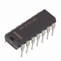
IC POT DIGITAL DUAL 10K 14-DIP
Manufacturer
Maxim Integrated Products
Datasheet
1.DS1868-10.pdf
(14 pages)
Specifications of DS1868-10+
Taps
256
Resistance (ohms)
10K
Number Of Circuits
2
Temperature Coefficient
750 ppm/°C Typical
Memory Type
Volatile
Interface
3-Wire Serial
Voltage - Supply
2.7 V ~ 3.3 V, 4.5 V ~ 5.5 V
Operating Temperature
-40°C ~ 85°C
Mounting Type
Through Hole
Package / Case
14-DIP (0.300", 7.62mm)
Resistance In Ohms
10K
Number Of Pots
Dual
Taps Per Pot
256
Resistance
10 KOhms
Wiper Memory
Volatile
Digital Interface
Serial (3-Wire)
Operating Supply Voltage
4.5 V to 5.5 V
Supply Current
1 uA
Maximum Operating Temperature
+ 85 C
Minimum Operating Temperature
- 40 C
Description/function
Dual Digital Potentiometer Chip
Mounting Style
SMD/SMT
Supply Voltage (max)
5.5 V
Supply Voltage (min)
4.5 V
Tolerance
20 %
Lead Free Status / RoHS Status
Lead free / RoHS Compliant


DS1868
DS1868 BLOCK DIAGRAM Figure 1
I/O SHIFT REGISTER Figure 2
Transmission of data always begins with the stack select bit followed by the potentiometer-1 wiper
position value and lastly the potentiometer-0 wiper position value.
When wiper position data is to be written to the DS1868, 17 bits (or some integer multiple) of data should
always be transmitted. Transactions which do not send a complete 17 bits (or multiple) will leave the
register incomplete and possibly an error in the desired wiper positions.
After a communication transaction has been completed the
signal input should be taken to a low
RST
state to prevent any inadvertent changes to the device shift register. Once
has reached a low state,
RST
the contents of the I/O shift register are loaded into the respective multiplexers for setting wiper position.
A new wiper position will only engage after a
transition to the inactive state. On device power-up,
RST
wiper position will be random.
STACKED CONFIGURATION
The potentiometers of the DS1868 can be connected in series as shown in Figure 3. This is referred to as
the stacked configuration and allows the user to double the total end-to-end resistance of the part. The
resolution of the combined potentiometers will remain the same as a single potentiometer but with a total
of 512 wiper positions available. Device resolution is defined as R
/256 (per potentiometer); where
TOT
R
equals the total potentiometer resistance.
TOT
The wiper output for the combined stacked potentiometer will be taken at the S
pin, which is the
OUT
multiplexed output of the wiper of potentiometer-0 (W0) or potentiometer-1 (W1). The potentiometer
wiper selected at the S
output is governed by the setting of the stack select bit (bit 0) of the 17-bit I/O
OUT
shift register. If the stack select bit has value 0, the multiplexed output, S
, will be that of the
OUT
3 of 14
Related parts for DS1868-10+
Image
Part Number
Description
Manufacturer
Datasheet
Request
R

Part Number:
Description:
IC POT DIGITAL DUAL 100K 14-DIP
Manufacturer:
Maxim Integrated Products
Datasheet:
Part Number:
Description:
IC POT DIGITAL DUAL 50K 14-DIP
Manufacturer:
Maxim Integrated Products
Datasheet:
Part Number:
Description:
IC POT DIGITAL DUAL 10K 14-DIP
Manufacturer:
Maxim Integrated Products
Datasheet:
Part Number:
Description:
IC POT DIGITAL DUAL 50K 14-DIP
Manufacturer:
Maxim Integrated Products
Datasheet:
Part Number:
Description:
IC POT DIGITAL DUAL 100K 14-DIP
Manufacturer:
Maxim Integrated Products
Datasheet:

Part Number:
Description:
Ds1868 Dual Digital Potentiometer Chip
Manufacturer:
Maxim Integrated Products, Inc.
Datasheet:

Part Number:
Description:
MAX7528KCWPMaxim Integrated Products [CMOS Dual 8-Bit Buffered Multiplying DACs]
Manufacturer:
Maxim Integrated Products
Datasheet:
Part Number:
Description:
Single +5V, fully integrated, 1.25Gbps laser diode driver.
Manufacturer:
Maxim Integrated Products
Datasheet:
Part Number:
Description:
Single +5V, fully integrated, 155Mbps laser diode driver.
Manufacturer:
Maxim Integrated Products
Datasheet:
Part Number:
Description:
VRD11/VRD10, K8 Rev F 2/3/4-Phase PWM Controllers with Integrated Dual MOSFET Drivers
Manufacturer:
Maxim Integrated Products
Datasheet:
Part Number:
Description:
Highly Integrated Level 2 SMBus Battery Chargers
Manufacturer:
Maxim Integrated Products
Datasheet:
Part Number:
Description:
Current Monitor and Accumulator with Integrated Sense Resistor; ; Temperature Range: -40°C to +85°C
Manufacturer:
Maxim Integrated Products
Part Number:
Description:
TSSOP 14/A°/RS-485 Transceivers with Integrated 100O/120O Termination Resis
Manufacturer:
Maxim Integrated Products
Part Number:
Description:
TSSOP 14/A°/RS-485 Transceivers with Integrated 100O/120O Termination Resis
Manufacturer:
Maxim Integrated Products
Part Number:
Description:
QFN 16/A°/AC-DC and DC-DC Peak-Current-Mode Converters with Integrated Step
Manufacturer:
Maxim Integrated Products