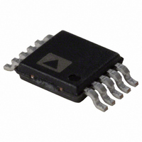
AD5161BRM100 Analog Devices Inc, AD5161BRM100 Datasheet - Page 18

AD5161BRM100
Manufacturer Part Number
AD5161BRM100
Description
IC POT DGTL 100K 256POS 10-MSOP
Manufacturer
Analog Devices Inc
Datasheet
1.AD5161BRMZ10.pdf
(20 pages)
Specifications of AD5161BRM100
Rohs Status
RoHS non-compliant
Taps
256
Resistance (ohms)
100K
Number Of Circuits
1
Temperature Coefficient
45 ppm/°C Typical
Memory Type
Volatile
Interface
I²C, SPI
Voltage - Supply
2.7 V ~ 5.5 V
Operating Temperature
-40°C ~ 125°C
Mounting Type
Surface Mount
Package / Case
10-MSOP, Micro10™, 10-uMAX, 10-uSOP
Resistance In Ohms
100K
Available stocks
Company
Part Number
Manufacturer
Quantity
Price
Part Number:
AD5161BRM100
Manufacturer:
ADI/亚德诺
Quantity:
20 000
AD5161
LEVEL SHIFTING FOR BIDIRECTIONAL INTERFACE
While most legacy systems may be operated at one voltage, a
new component may be optimized at another. When two systems
operate the same signal at two different voltages, proper level
shifting is needed. For instance, one can use a 3.3 V E
interface with a 5 V digital potentiometer. A level shifting scheme is
needed to enable a bidirectional communication so that the setting
of the digital potentiometer can be stored to and retrieved from
the E
and M2 can be any N-channel signal FETs, or if V
2.5 V, low threshold FETs such as the FDV301N.
ESD PROTECTION
All digital inputs are protected with a series input resistor and
parallel Zener ESD structures shown in Figure 46 and Figure 47.
This applies to the digital input pins SDI/SDA, CLK/SCL, and
CS /AD0.
V
SDA1
2
SCL1
DD1
PROM. Figure 45 shows one of the implementations. M1
Figure 45. Level Shifting for Operation at Different Potentials
= 3.3V
Figure 47. ESD Protection of Resistor Terminals
E
2
PROM
3.3V
Figure 46. ESD Protection of Digital Pins
R
P
R
A,B,W
P
S
340Ω
G
M1
V ss
V
SS
D
S
G
M2
LOGIC
D
R
P
AD5161
R
P
5V
V
DD2 =
DD
falls below
5V
2
PROM to
SDA2
SCL2
Rev. A | Page 18 of 20
TERMINAL VOLTAGE OPERATING RANGE
The AD5161 V
conditions for proper 3-terminal digital potentiometer
operation. Supply signals present on terminals A, B, and W that
exceed V
biased diodes (see Figure 48).
POWER-UP SEQUENCE
Since the ESD protection diodes limit the voltage compliance at
terminals A, B, and W (see Figure 48), it is important to power
V
otherwise, the diode will be forward biased such that V
be powered unintentionally and may affect the rest of the user’s
circuit. The ideal power-up sequence is in the following order:
GND, V
powering V
long as they are powered after V
LAYOUT AND POWER SUPPLY BYPASSING
It is a good practice to employ compact, minimum lead length
layout design. The leads to the inputs should be as direct as
possible with a minimum conductor length. Ground paths
should have low resistance and low inductance.
Similarly, it is also a good practice to bypass the power supplies
with quality capacitors for optimum stability. Supply leads to
the device should be bypassed with disc or chip ceramic
capacitors of 0.01 μF to 0.1 μF. Low ESR 1 μF to 10 μF tantalum
or electrolytic capacitors should also be applied at the supplies
to minimize any transient disturbance and low frequency ripple
(see Figure 49). Note that the digital ground should also be
joined remotely to the analog ground at one point to minimize
the ground bounce.
DD
/GND before applying any voltage to terminals A, B, and W;
Figure 48. Maximum Terminal Voltages Set by V
DD
DD
, digital inputs, and then V
or GND will be clamped by the internal forward
A
, V
V
DD
DD
B
, V
C3
Figure 49. Power Supply Bypassing
and GND power supply defines the boundary
W
+
, and the digital inputs is not important as
10μF
C1
0.1μF
DD
/GND.
V
A/B/W
DD
AD5161
. The relative order of
GND
DD
V
V
and V
W
A
B
DD
SS
SS
DD
will


