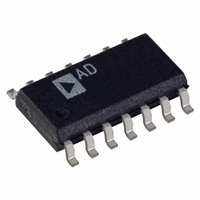
AD5241BR1M Analog Devices Inc, AD5241BR1M Datasheet - Page 7

AD5241BR1M
Manufacturer Part Number
AD5241BR1M
Description
IC DGTL POT 256POS 14-SOIC
Manufacturer
Analog Devices Inc
Datasheet
1.AD5242BRUZ100-RL7.pdf
(20 pages)
Specifications of AD5241BR1M
Mounting Type
Surface Mount
Package / Case
14-SOIC (3.9mm Width), 14-SOL
Rohs Status
RoHS non-compliant
Taps
256
Resistance (ohms)
1M
Number Of Circuits
1
Temperature Coefficient
30 ppm/°C Typical
Memory Type
Volatile
Interface
I²C, 2-Wire Serial
Voltage - Supply
2.7 V ~ 5.5 V, ±2.3 V ~ 2.7 V
Operating Temperature
-40°C ~ 105°C
Resistance In Ohms
1.00M
Ic Function
Digital Potentiometer (Pots) IC
Lead Free Status / RoHS Status
PIN CONFIGURATIONS AND FUNCTION DESCRIPTIONS
Table 4. AD5241 Pin Function Descriptions
Pin No.
1
2
3
4
5
6
7
8
9
10
11
12
13
14
Mnemonic
A
W
B
V
SHDN
SCL
SDA
AD0
AD1
DGND
V
O
NC
O
1
DD
SS
1
2
1
1
Figure 6. AD5241 Pin Configuration
SHDN
SDA
SCL
V
W
A
B
DD
1
1
1
NC = NO CONNECT
1
2
3
4
5
6
7
Serial Clock Input.
Common Ground.
No Connect.
Description
Resistor Terminal A
Wiper Terminal W
Resistor Terminal B
Positive Power Supply, Specified for
Operation from 2.2 V to 5.5 V.
Active low, asynchronous connection of
Wiper W to Terminal B, and open circuit
of Terminal A. RDAC register contents
unchanged. SHDN should tie to V
if not used.
Serial Data Input/Output.
Programmable Address Bit for Multiple
Package Decoding. Bit AD0 and Bit AD1
provide four possible addresses.
Programmable Address Bit for Multiple
Package Decoding. Bit AD0 and Bit AD1
provide four possible addresses.
Negative Power Supply, Specified for
Operation from 0 V to −2.7 V.
Logic Output Terminal O
Logic Output Terminal O
(Not to Scale)
AD5241
TOP VIEW
14
13
12
11
10
9
8
O
NC
O
V
DGND
AD1
AD0
SS
1
2
1
.
1
1
.
.
2
1
.
.
DD
Rev. C | Page 7 of 20
Table 5. AD5242 Pin Function Descriptions
Pin No.
1
2
3
4
5
6
7
8
9
10
11
12
13
14
15
16
Mnemonic
O
A
W
B
V
SHDN
SCL
SDA
AD0
AD1
DGND
V
O
B
W
A
1
DD
SS
2
1
2
1
2
1
2
Figure 7. AD5242 Pin Configuration
SHDN
SDA
SCL
V
W
O
A
B
DD
1
1
1
1
1
2
3
4
5
6
7
8
Description
Logic Output Terminal O
Resistor Terminal A
Wiper Terminal W
Resistor Terminal B
Positive Power Supply, Specified for
Operation from 2.2 V to 5.5 V.
Active Low, Asynchronous Connection
of Wiper W to Terminal B, and Open
Circuit of Terminal A. RDAC register
contents unchanged. SHDN should
tie to V
Serial Clock Input.
Serial Data Input/Output.
Programmable Address Bit for Multiple
Package Decoding. Bit AD0 and Bit AD1
provide four possible addresses.
Programmable Address Bit for Multiple
Package Decoding. Bit AD0 and Bit AD1
provide four possible addresses.
Common Ground.
Negative Power Supply, Specified for
Operation from 0 V to −2.7 V.
Logic Output Terminal O
Resistor Terminal B
Wiper Terminal W
Resistor Terminal A
(Not to Scale)
AD5242
TOP VIEW
DD
, if not used.
16
15
14
13
12
10
11
9
AD5241/AD5242
A
W
B
O
V
DGND
AD1
AD0
SS
2
2
2
2
1
2
.
.
1
2
1
2
.
.
.
.
1
2
.
.


