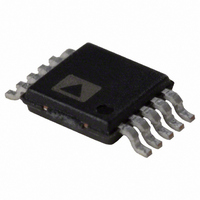
AD5172BRM10 Analog Devices Inc, AD5172BRM10 Datasheet - Page 8

AD5172BRM10
Manufacturer Part Number
AD5172BRM10
Description
IC POT DUAL 10K 256POS 10-MSOP
Manufacturer
Analog Devices Inc
Datasheet
1.AD5172BRMZ2.5.pdf
(24 pages)
Specifications of AD5172BRM10
Rohs Status
RoHS non-compliant
Taps
256
Resistance (ohms)
10K
Number Of Circuits
2
Temperature Coefficient
35 ppm/°C Typical
Memory Type
Non-Volatile
Interface
I²C, 2-Wire Serial
Voltage - Supply
2.7 V ~ 5.5 V
Operating Temperature
-40°C ~ 125°C
Mounting Type
Surface Mount
Package / Case
10-MSOP, Micro10™, 10-uMAX, 10-uSOP
Resistance In Ohms
10K
Available stocks
Company
Part Number
Manufacturer
Quantity
Price
Company:
Part Number:
AD5172BRM100-RL7
Manufacturer:
AD
Quantity:
1 100
AD5172/AD5173
PIN CONFIGURATIONS AND FUNCTION DESCRIPTIONS
Table 5. AD5172 Pin Function Descriptions
Pin
No.
1
2
3
4
5
6
7
8
9
10
Mnemonic
B1
A1
W2
GND
V
SCL
SDA
A2
B2
W1
DD
Figure 4. AD5172 Pin Configuration
GND
V
W2
B1
A1
DD
Description
B1 Terminal. GND ≤ V
A1 Terminal. GND ≤ V
W2 Terminal. GND ≤ V
Digital Ground.
Positive Power Supply. Specified for
operation from 2.7 V to 5.5 V. For OTP
programming, V
of 5.6 V but no more than 5.8 V and to be
capable of driving 100 mA.
Serial Clock Input. Positive-edge triggered.
Requires a pull-up resistor. If this pin is driven
directly from a logic controller without a
pull-up resistor, ensure that the V
is 0.7 V × V
Serial Data Input/Output. Requires a pull-up
resistor. If this pin is driven directly from a
logic controller without a pull-up resistor,
ensure that the V
A2 Terminal. GND ≤ V
B2 Terminal. GND ≤ V
W1 Terminal. GND ≤ V
1
2
3
4
5
(Not to Scale)
AD5172
TOP VIEW
DD
.
DD
IH
10
9
8
7
6
needs to be a minimum
minimum is 0.7 V × V
W1
B2
A2
SDA
SCL
B1
B2
A1
A2
W2
W1
≤ V
≤ V
≤ V
≤ V
≤ V
≤ V
DD
DD
DD
DD
DD
DD
.
.
.
.
.
.
IH
minimum
DD
Rev. H | Page 8 of 24
.
Table 6. AD5173 Pin Function Descriptions
Pin
No.
1
2
3
4
5
6
7
8
9
10
Mnemonic
B1
AD0
W2
GND
V
SCL
SDA
AD1
B2
W1
DD
Figure 5. AD5173 Pin Configuration
GND
AD0
V
W2
B1
DD
Description
B1 Terminal. GND ≤ V
Programmable Address Bit 0 for Multiple
Package Decoding.
W2 Terminal. GND ≤ V
Digital Ground.
Positive Power Supply. Specified for
operation from 2.7 V to 5.5 V. For OTP
programming, V
of 5.6 V but no more than 5.8 V and to be
capable of driving 100 mA.
Serial Clock Input. Positive-edge triggered.
Requires a pull-up resistor. If this pin is driven
directly from a logic controller without a
pull-up resistor, ensure that the V
is 0.7 V × V
Serial Data Input/Output. Requires a pull-up
resistor. If this pin is driven directly from a
logic controller without a pull-up resistor,
ensure that the V
Programmable Address Bit 1 for Multiple
Package Decoding.
B2 Terminal. GND ≤ V
W1 Terminal. GND ≤ V
1
2
3
4
5
(Not to Scale)
AD5173
TOP VIEW
DD
.
DD
IH
10
9
8
7
6
needs to be a minimum
minimum is 0.7 V × V
W1
B2
AD1
SDA
SCL
B1
B2
W2
W1
≤ V
≤ V
≤ V
≤ V
DD
DD
DD
DD
.
.
.
.
IH
minimum
DD
.


