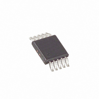
DS3502U+ Maxim Integrated Products, DS3502U+ Datasheet

DS3502U+
Specifications of DS3502U+
Related parts for DS3502U+
DS3502U+ Summary of contents
Page 1
... Digital Operating Voltage: 2.5V to 5.5V ♦ Analog Operating Voltage: 4.5V to 15.5V Applications ♦ Operating Temperature: -40°C to +100°C ♦ 10-Pin µSOP Package PART DS3502U+ DS3502U+T&R + Denotes a lead(Pb)-free/RoHS-compliant package. T&R = Tape and reel. 7-BIT WIPER REGISTER DS3502 DECODER LEVEL SHIFTER ...
Page 2
High-Voltage, NV, I ABSOLUTE MAXIMUM RATINGS Voltage Range on V Relative to GND ...............-0.5V to +6.0V CC Voltage Range on V+ Relative to GND ..................-0.5V to +17V Voltage Range on SDA, SCL, A0, A1 Relative to GND.......-0. ...
Page 3
VOLTAGE-DIVIDER CHARACTERISTICS (V = +2.5V to +5.5V -40°C to +100°C, unless otherwise noted PARAMETER SYMBOL Integral Nonlinearity Differential Nonlinearity Zero-Scale Error ZS Full-Scale Error FS Ratiometric Temp Coefficient ELECTRICAL CHARACTERISTICS (V = ...
Page 4
High-Voltage, NV, I NONVOLATILE MEMORY CHARACTERISTICS (V = +2.5V to +5.5V) CC PARAMETER SYMBOL EEPROM Write Cycles Note 1: All voltages are referenced to ground. Currents entering the IC are specified positive and currents exiting the IC are negative. Note ...
Page 5
A A SUPPLY CURRENT vs. SUPPLY VOLTAGE 1.8 SDA = SCL = V CC 1.6 RW, RH, AND RL ARE FLOATING 1.4 1.2 1.0 0.8 0.6 0.4 0.2 ...
Page 6
High-Voltage, NV GND SCL INTERFACE SDA A0 A1 Detailed Description The DS3502 contains a single potentiometer whose wiper position is controlled by the value in the Wiper Register (WR). The initial power-up value of ...
Page 7
Slave Address Byte and Address Pins The slave address byte consists of a 7-bit slave address plus a R/W bit (see Figure 1). The DS3502’s slave address is determined by the state of the A0 and A1 address pins. These ...
Page 8
High-Voltage, NV, I data bit is valid at the rising edge of the current SCL pulse. Remember that the master generates all SCL clock pulses, including when it is reading bits from the slave. Acknowledge (ACK and NACK): An Acknowledge ...
Page 9
TYPICAL I C WRITE TRANSACTION MSB LSB START R/W READ/ SLAVE WRITE ADDRESS* 2 EXAMPLE I C TRANSACTIONS (WHEN A0 AND A1 ARE CONNECTED TO GND). 50h A) SINGLE-BYTE WRITE 0 1 ...
Page 10
High-Voltage, NV GATE 1 C STOR GATE 2 GATE 3 2. SDA SCL DS3502 A0 A1 GND Pin Configuration TOP VIEW SDA 1 GND DS3502 ...
Page 11
... Maxim cannot assume responsibility for use of any circuitry other than circuitry entirely embodied in a Maxim product. No circuit patent licenses are implied. Maxim reserves the right to change the circuitry and specifications without notice at any time. Maxim Integrated Products, 120 San Gabriel Drive, Sunnyvale, CA 94086 408-737-7600 ____________________ 11 © 2009 Maxim Integrated Products ...


