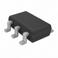
MAX5435LEZT+T Maxim Integrated Products, MAX5435LEZT+T Datasheet - Page 9

MAX5435LEZT+T
Manufacturer Part Number
MAX5435LEZT+T
Description
IC POT DGTL 32TAP NV TSOT23-6
Manufacturer
Maxim Integrated Products
Datasheet
1.MAX5434LEZTT.pdf
(19 pages)
Specifications of MAX5435LEZT+T
Taps
32
Resistance (ohms)
100K
Number Of Circuits
1
Temperature Coefficient
35 ppm/°C Typical
Memory Type
Non-Volatile
Interface
I²C, 2-Wire Serial
Voltage - Supply
2.7 V ~ 5.25 V
Operating Temperature
-40°C ~ 85°C
Mounting Type
Surface Mount
Package / Case
TSOT-23-6, TSOT-6
Resistance In Ohms
100K
Lead Free Status / RoHS Status
Lead free / RoHS Compliant
high while SCL is high. The bus is then free for another
transmission (Figure 3).
One data bit is transferred during each clock pulse.
The data on the SDA line must remain stable while SCL
is high (Figure 5).
The acknowledge bit is a clocked 9th bit that the recip-
ient uses to handshake receipt of each byte of data
(Figure 6). Each byte transferred effectively requires 9
bits. The master generates the 9th clock pulse, and the
recipient pulls down SDA during the acknowledge
clock pulse, so the SDA line is stable low during the
high period of the clock pulse. When the master trans-
mits to the MAX5432–MAX5435, the devices generate
the acknowledge bit because the MAX5432–MAX5435
are the recipients.
The MAX5432–MAX5435 have a 7-bit-long slave
address (Figure 4). The 8th bit following the 7-bit slave
address is the
write command and high for a no-operation command.
Table 1a shows four possible slave addresses for the
MAX5432/MAX5433 and Table 1b shows three possible
slave addresses for the MAX5434/MAX5435. The first 4
bits (MSBs) of the slave addresses are always 0101.
Bits A2 and A1 are factory programmed for the
MAX5432/MAX5433 (Table 1a). Connect the A0 input
(MAX5432/MAX5433 only) to either GND or V
select one of two I
must have a unique address to share the bus. A maxi-
mum of four MAX5432/MAX5433 devices can share the
same bus. Bits A2, A1, and A0 are factory programmed
for the MAX5434/MAX5435 (Table 1b).
Figure 1. I
PARAMETERS ARE MEASURED FROM 30% TO 70%.
SDA
SCL
S
2
C Serial-Interface Timing Diagram
t
SU-DAT
t
HD-STA
t
NOP/W bit. Set the NOP/W bit low for a
LOW
_______________________________________________________________________________________
2
C device addresses. Each device
t
R
32-Tap, Nonvolatile, I
t
HIGH
t
F
t
HD-DAT
Slave Address
Acknowledge
Bit Transfer
DD
t
SU-STA
to
A write to the MAX5432–MAX5435 consists of the trans-
mission of the device’s slave address with the 8th bit set
to zero, followed by at least 1 byte of information. The
1st byte of information is the command byte. The bytes
received after the command byte are the data bytes.
The 1st data byte goes into the internal register of the
MAX5432–MAX5435 as selected by the command byte
(Figure 8).
Table 1a. Address Codes
(MAX5432/MAX5433 Only)
Table 1b. Address Codes
(MAX5434/MAX5435 Only)
*MAX5434 only.
SUFFIX
SUFFIX
PART
Sr
PART
M
M
L
L
M
N*
L
t
HD-STA
A6
A6
0
0
0
0
0
0
0
2
C, Linear, Digital
A5
A5
A
1
1
1
1
1
1
1
Potentiometers
Message Format for Writing
A4
A4
0
0
0
0
0
0
0
ADDRESS BYTE
ADDRESS BYTE
A3
A3
1
1
1
1
1
1
1
t
SU-STO
A2
A2
0
0
1
1
0
1
0
A1
A1
0
0
0
0
t
0
0
1
R
P
t
BUF
A0
A0
0
1
0
1
0
0
0
t
F
NOP/W
NOP/W
NOP/W
NOP/W
NOP/W
S
NOP/W
NOP/W
NOP/W
NOP/W
9


