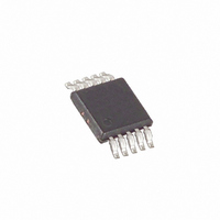
DS3905U-020 Maxim Integrated Products, DS3905U-020 Datasheet - Page 10

DS3905U-020
Manufacturer Part Number
DS3905U-020
Description
IC POT NV TRIPLE 128POS 10-USOP
Manufacturer
Maxim Integrated Products
Datasheet
1.DS3904U-020.pdf
(11 pages)
Specifications of DS3905U-020
Taps
128
Resistance (ohms)
20K
Number Of Circuits
3
Memory Type
Non-Volatile
Interface
I²C, 2-Wire Serial
Voltage - Supply
2.7 V ~ 5.5 V
Operating Temperature
-40°C ~ 85°C
Mounting Type
Surface Mount
Package / Case
10-MSOP, Micro10™, 10-uMAX, 10-uSOP
Resistance In Ohms
20K
Lead Free Status / RoHS Status
Contains lead / RoHS non-compliant
Temperature Coefficient
-
Available stocks
Company
Part Number
Manufacturer
Quantity
Price
Part Number:
DS3905U-020+
Manufacturer:
MAXIM/美信
Quantity:
20 000
Triple 128-Position Nonvolatile Digital
Variable Resistor/Switch
Figure 4. Command and Data Byte Structures
Figure 5. Example 2-Wire Transactions
10
START
*DS3904, USE 0's INSTEAD OF A2 AND A1 FOR THE DEVICE ADDRESS
one clock pulse per bit of data. Figures 2 and 3
detail how data transfer is accomplished on the 2-
wire bus. Depending upon the state of the R/W bit,
two types of data transfer are possible.
Each data transfer is initiated with a start condition
and terminated with a stop condition. The number
of data bytes transferred between start and stop
conditions is not limited and is determined by the
master device. The information is transferred byte-
wise and each receiver acknowledges with a ninth
bit.
Within the bus specifications, a regular mode
(100kHz clock rate) and a fast mode (400kHz clock
rate) are defined. The DS3904/DS3905 work in both
modes.
Acknowledge: Each receiving device, when
addressed, generates an acknowledge after the
byte has been received. The master device must
generate an extra clock pulse that is associated
with this acknowledge bit.
_____________________________________________________________________
READ RESISTOR 1 VALUE
SET RESISTOR 1 TO Hi-Z
MSB
WRITE RESISTOR 2 TO
1
DEVICE IDENTIFIER
EXAMPLE 2-WIRE TRANSACTIONS
A0 = GND FOR DS3904
A0, A1, A2 = GND FOR DS3905
"FAMILY CODE"
WRITE RESISTOR 0
TO MIN POSITION
0
MAX POSITION
OR
COMMAND BYTE
1
0
A2* A1* A0 R/W
ADDRESS
START
START
START
START
SLAVE
MSB
MSB
MSB
MSB
MSB
1
1
1
1
1
LSB
0
0
0
0
0
1
1
1
1
1
CONTROL BIT
MSB
RHIZ
0
0
0
0
0
A0h
A0h
A0h
A0h
A1h
0
0
0
0
0
0
0
0
0
0
DATA BYTE
RESISTOR SETTING
0
0
0
0
0
LSB
LSB
LSB
LSB
LSB
0
0
0
0
1
FROM
SLAVE
ACK
ACK
ACK
ACK
ACK
LSB
MSB
MSB
MSB
MSB
MSB
1
1
1
1
1
1
1
1
1
1
1
1
RESISTOR DATA
1
1
1
1
F8h
F9h
FAh
F9h
1
1
1
1
A device that acknowledges must pull down the
SDA line during the acknowledge clock pulse in
such a way that the SDA line is a stable low during
the high period of the acknowledge-related clock
pulse. Of course, setup and hold times must be
taken into account. A master must signal an end of
data to the slave by not generating an acknowl-
edge bit on the last byte that has been clocked out
of the slave. In this case, the slave must leave the
data line high to enable the master to generate the
stop condition.
Data transfer from a master transmitter to a
slave receiver. The first byte transmitted by the
master is the command/control byte. Next follows a
number of data bytes. The slave returns an
acknowledge bit after each received byte.
Data transfer from a slave transmitter to a mas-
ter receiver. The master transmits the first byte (the
command/control byte) to the slave. The slave then
returns an acknowledge bit. Next follows the data
byte transmitted by the slave to the master. The
master returns NACK followed by a stop.
The master device generates all serial clock pulses
and the start and stop conditions. A transfer is
ended with a stop condition or with a repeated start
condition. Since a repeated start condition is also
the beginning of the next serial transfer, the bus is
not released.
0
0
0
0
0
0
1
0
LSB
LSB
LSB
LSB
LSB
0
1
0
1
MASTER
FROM
SLAVE
NACK
ACK
ACK
ACK
ACK
MSB
MSB
MSB
STOP
0
1
0
REPEATED
START
0
0
1
0
0
1
0
0
1
00h
80h
7Fh
0
0
1
0
0
1
0
0
1
LSB
LSB
LSB
0
0
1
FROM
SLAVE
ACK
ACK
ACK
STOP
STOP
STOP


