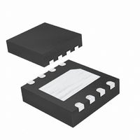
MAX5417META+T Maxim Integrated Products, MAX5417META+T Datasheet - Page 13

MAX5417META+T
Manufacturer Part Number
MAX5417META+T
Description
IC POT DGTL 256-TAP I2C 8-TDFN
Manufacturer
Maxim Integrated Products
Datasheet
1.MAX5418LETAT.pdf
(14 pages)
Specifications of MAX5417META+T
Taps
256
Resistance (ohms)
50K
Number Of Circuits
1
Temperature Coefficient
35 ppm/°C Typical
Memory Type
Non-Volatile
Interface
I²C, 2-Wire Serial
Voltage - Supply
2.7 V ~ 5.25 V
Operating Temperature
-40°C ~ 85°C
Mounting Type
Surface Mount
Package / Case
8-TDFN Exposed Pad
Resistance In Ohms
50K
Number Of Pots
Single
Taps Per Pot
256
Resistance
50 KOhms
Wiper Memory
Non Volatile
Digital Interface
Serial (2-Wire, I2C)
Operating Supply Voltage
5 V
Supply Current
0.001 mA
Maximum Operating Temperature
+ 85 C
Minimum Operating Temperature
- 40 C
Description/function
50kOhm, 256-Tap, Nonvolatile, I2C-Interface Digital Potentiometer
Mounting Style
SMD/SMT
Supply Voltage (max)
5.25 V
Supply Voltage (min)
2.7 V
Lead Free Status / RoHS Status
Lead free / RoHS Compliant
Figure 11. Programmable Filter
Figure 12. Adjustable Voltage Reference
Figure 12 shows the MAX5417/MAX5418/MAX5419 used
as the feedback resistors in multiple adjustable voltage-
reference applications. Independently adjust the output
voltage of the MAX6160 from 1.23V to V
changing the wiper positions of the MAX5417/
MAX5418/MAX5419.
Connect the high and low terminals of one potentiometer
of a MAX5417 between the NULL inputs of a MAX410
and the wiper to the op amp’s positive supply to nullify
the offset voltage over the operating temperature range.
Install the other potentiometer in the feedback path to
adjust the gain of the MAX410 (see Figure 13).
V
MAX5417
MAX5418
MAX5419
Offset Voltage and Gain Adjustment
IN
MAX5417
MAX5418
MAX5419
H
Adjustable Voltage Reference
R3
______________________________________________________________________________________
W
L
MAX6160
GND
+5V
V
IN
R2
C
H
L
OUT
256-Tap, Nonvolatile, I
ADJ
W
W
R1
H
L
V
0
REF
IN
V
OUT
- 0.2V by
For the latest package outline information and land patterns, go
to www.maxim-ic.com/packages. Note that a “+”, “#”, or “-” in
the package code indicates RoHS status only. Package draw-
ings may show a different suffix character, but the drawing per-
tains to the package regardless of RoHS status.
Figure 13. Offset Voltage and Gain Adjustment Circuit
PROCESS: BiCMOS
Digital Potentiometers
PACKAGE TYPE
8 TDFN-EP
TOP VIEW
L
W
SDA
SCL
V
R1
DD
A0
PACKAGE CODE
1
2
4
+
3
Package Information
2
H
3
2
T833-1
MAX5417
MAX5418
MAX5419
7
C-Interface,
-5V
TDFN
5V
Pin Configuration
MAX410
Chip Information
4
1
8
6
8
7
5
DOCUMENT NO.
H
W
L
GND
6
MAX5417
MAX5418
MAX5419
21-0137
13


