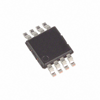
MAX5420BEUA+ Maxim Integrated Products, MAX5420BEUA+ Datasheet - Page 6

MAX5420BEUA+
Manufacturer Part Number
MAX5420BEUA+
Description
IC VOLTAGE DIVIDER DGLT 8-UMAX
Manufacturer
Maxim Integrated Products
Datasheet
1.MAX5420AEUA.pdf
(9 pages)
Specifications of MAX5420BEUA+
Taps
4
Resistance (ohms)
15K
Number Of Circuits
1
Memory Type
Volatile
Interface
2-Wire Parallel
Voltage - Supply
4.75 V ~ 5.25 V, ±0.0 V ~ 5.25 V
Operating Temperature
-40°C ~ 85°C
Mounting Type
Surface Mount
Package / Case
8-MSOP, Micro8™, 8-uMAX, 8-uSOP,
Resistance In Ohms
15K
Lead Free Status / RoHS Status
Lead free / RoHS Compliant
Temperature Coefficient
-
The MAX5420/MAX5421 are digitally programmable pre-
cision voltage dividers for programmable-gain amplifiers.
Operationally, these devices consist of digitally selectable
precision resistor-dividers providing noninverting gains of
1, 2, 4, and 8 for PGA applications (see Functional
Diagram and Figure 1).
The MAX5420/MAX5421 achieve divider ratio accuracy of
0.025% (MAX5420A/MAX5421A), 0.09% (MAX5420B/
MAX5421B) or 0.5% (MAX5420C/MAX5421C).
The end-to-end resistance from H to L is 15k . The
impedance seen at W is designed to be the same 8k
for divider ratios 2, 4, and 8, ensuring excellent imped-
ance matching and constant switching times. In gain of
+1 configuration, H is internally connected to W with a
typical resistance of 500 .
The MAX5421 includes a matching resistor to compen-
sate for offset voltage due to input bias current of the
op amp. The resistance from MATCH_H to MATCH_L,
equals the resistance seen at W for gains of 2, 4, and 8.
In the gain of +1, an internal switch connects
MATCH_H and MATCH_L. This internal switch matches
the impedance of the switch between H and W.
Digitally Programmable Precision
Voltage Divider for PGAs
6
MAX5420
_______________________________________________________________________________________
4, 5
—
—
1
2
3
6
7
8
PIN
MAX5421
Matching Resistor (MAX5421)
4, 5
10
Ratio
1
2
3
8
9
6
7
Detailed Description
1
MATCH_H
MATCH_L
D0, D1
NAME
R A
R B
GND
V
V
W
_
H
_
DD
SS
L
Positive Supply Voltage
Negative Supply Voltage
Ground
Digital Control Inputs. Drive D0 and D1 logic high or logic low to set the divider ratio.
See Logic Control Truth Table.
Low Terminal of Resistor-Divider
Resistor-Divider Output
High Terminal of Resistor-Divider
Matching Resistor Low Terminal
Matching Resistor High Terminal
The MAX5420/MAX5421 feature a simple two-bit paral-
lel programming interface. D1 and D0 program the
divider ratio setting according to the Logic Control
Truth Table (Table 1). The digital interface is CMOS/TTL
logic compatible.
The MAX5420/MAX5421 are ideally suited for high-pre-
cision PGA applications. The typical application circuit
of Figure 3 uses the MAX5421 with matching resistor to
compensate for voltage offset due to op amp input bias
currents. Use the MAX5420 with an ultra-low input bias
current op amp such as the MAX4237 (Figure 4).
The MAX5420/MAX5421 operate from dual ±5V sup-
plies, or a single +5V supply. For dual supplies, bypass
V
For single supply, connect V
V
Table 1. Logic Control Truth Table
DD
DD
with a 0.1µF ceramic capacitor to GND.
and V
D1
0
0
1
1
DIGITAL INPUTS
SS
FUNCTION
with 0.1µF ceramic capacitors to GND.
Applications Information
Power Supplies and Bypassing
Programmable-Gain Amplifier
Digital Interface Operation
D0
0
1
0
1
SS
Pin Description
to GND and bypass
DIVIDER
RATIO
1
2
4
8


