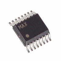
MAX5411EEE+ Maxim Integrated Products, MAX5411EEE+ Datasheet - Page 8

MAX5411EEE+
Manufacturer Part Number
MAX5411EEE+
Description
IC POT DGTL DUAL AUDIO 16-QSOP
Manufacturer
Maxim Integrated Products
Datasheet
1.MAX5408EEE.pdf
(13 pages)
Specifications of MAX5411EEE+
Taps
32
Resistance (ohms)
10K
Number Of Circuits
2
Temperature Coefficient
35 ppm/°C Typical
Memory Type
Volatile
Interface
SPI, 3-Wire Serial
Voltage - Supply
4.5 V ~ 5.5 V
Operating Temperature
-40°C ~ 85°C
Mounting Type
Surface Mount
Package / Case
16-QSOP
Resistance In Ohms
10K
Lead Free Status / RoHS Status
Lead free / RoHS Compliant
The digital output, DOUT, lags the digital input signal,
DIN by 8.5 clock cycles. Force CS high to disable
DOUT, placing DOUT in three-state mode. Force CS
low to enable DOUT and disable three-state mode.
Force CS high, after a word has been written to the
MAX5408–MAX5411 to make a readback request. The
next CS low period writes the requested data to DOUT.
Dual, Audio, Log Taper Digital Potentiometers
Table 5. Zero-Crossing Detection Register Bit Definitions for MAX5408/MAX5410
Table 6. Zero-Crossing Detection Register Bit Definitions for MAX5409/MAX5411
Table 7. Attenuation and Wiper Position
8
_______________________________________________________________________________________
DATA BIT
DATA BIT
D4
D3
D2
D1
D0
D4
D3
D2
D1
D0
POSITION
MUTE
30
31
0
1
2
3
4
. .
. .
.
“don’t care”
“don’t care”
“don’t care”
“don’t care”
VALUE
VALUE
0
1
0
1
0
1
0
1
0
1
0
1
OUTPUT LEVEL (dB)
Disable wiper W0A zero-crossing detection circuit
Enable wiper W0A zero-crossing detection circuit
Disable wiper W0B zero-crossing detection circuit
Enable wiper W0B zero-crossing detection circuit
Disable wiper W1A zero-crossing detection circuit
Enable wiper W1A zero-crossing detection circuit
Disable wiper W1B zero-crossing detection circuit
Enable wiper W1B zero-crossing detection circuit
No change
Disable wiper W0A zero-crossing detection circuit
Enable wiper W0A zero-crossing detection circuit
No change
Disable wiper W1A zero-crossing detection circuit
Enable wiper W1A zero-crossing detection circuit
No change
No change
<-90
-60
-62
-2
-4
-6
-8
0
. .
. .
.
A readback request overwrites any previous data in the
shift register. Note that the data appears at DOUT in
the order: A0, A1, A2, D4, D3, D2, D1, D0. A0 will be
available after the first high-to-low transition of SCLK
when CS is low. The input continues to load the shift
register while data is being read out of the MAX5408–
MAX5411. The input data appears at DOUT 8.5 clock
cycles later. A CS transition from low-to-high latches
the input data. For any control byte, the state of SCLK
must be the same for both CS low-to-high transitions
and CS high-to-low transitions in order to preserve the
data at DOUT while CS transitions. For proper opera-
tion, ensure that the input data remains valid on both
the SCLK rising and falling edges when daisy chaining
multiple devices.
The zero-crossing detection register enables the zero-
crossing detect feature. The zero-crossing detect fea-
ture reduces the audible noise (“clicks and pops”) that
result from wiper transitions. The wiper changes posi-
tion only when the voltage at L_ is the same as the volt-
age at H_. Each wiper has a zero-crossing and timeout
FUNCTION
FUNCTION
Zero-Crossing Detection


