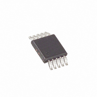
MAX5431AEUB+T Maxim Integrated Products, MAX5431AEUB+T Datasheet - Page 6

MAX5431AEUB+T
Manufacturer Part Number
MAX5431AEUB+T
Description
IC VOLTAGE DIVIDER PGA 10-UMAX
Manufacturer
Maxim Integrated Products
Datasheet
1.MAX5430BEKAT.pdf
(7 pages)
Specifications of MAX5431AEUB+T
Taps
4
Resistance (ohms)
57K
Number Of Circuits
1
Memory Type
Volatile
Interface
2-Wire Parallel
Voltage - Supply
12 V ~ 15 V, ±12 V ~ 15 V
Operating Temperature
-40°C ~ 85°C
Mounting Type
Surface Mount
Package / Case
10-MSOP, Micro10™, 10-uMAX, 10-uSOP
Resistance In Ohms
57K
Lead Free Status / RoHS Status
Lead free / RoHS Compliant
Temperature Coefficient
-
±15V Digitally Programmable
Precision Voltage-Dividers for PGAs
The MAX5430/MAX5431 feature a simple two-bit paral-
lel programming interface. D1 and D0 program the gain
setting according to the Logic-Control Truth Table (see
Table 1). The digital interface is CMOS/TTL logic com-
patible.
The MAX5430/MAX5431 are ideally suited for high-pre-
cision PGA applications. The typical application circuit
of Figure 2 uses the MAX5431 with matching resistor to
compensate for voltage offset due to op amp input bias
currents. Use the MAX5430 with an ultra-low input bias
current op amp (see Figure 3).
The MAX5430/MAX5431 operate from dual ±15V sup-
plies or a single 15V supply. For dual supplies, bypass
V
For single supply, connect V
V
The switching time of the MAX5430/MAX5431 depends
on the capacitive loading at W. For best performance,
reduce parasitic board capacitance by minimizing the
circuit board trace from W to the op amp inverting input,
and choose an op amp with low input capacitance.
Figure 2. MAX5431 Typical Application Circuit PGA with Input
I
6
BIAS
DD
DD
MATCH_H
_______________________________________________________________________________________
V
with a 0.1µF ceramic capacitor to GND.
Matching
and V
IN
Switching Time and Layout Concerns
SS
V
15V
SS
MAX5431
V
with 0.1µF ceramic capacitors to GND.
DD
Applications Information
Power Supplies and Bypassing
L
Programmable-Gain Amplifier
Digital Interface Operation
GND
SS
MATCH_L
W
H
to GND and bypass
15V
V
OUT
Figure 3. Programmable-Gain Amplifier Using the MAX5430
TRANSISTOR COUNT: 121
PROCESS: CMOS
Pin Configurations (continued)
TOP VIEW
V
V
D0
D1
SS
W
SS
15V
1
2
4
3
V
DD
L
MAX5430
GND
V
MAX5430
SOT23
IN
W
Chip Information
H
15V
6
8
7
5
V
L
GND
H
DD
V
OUT


