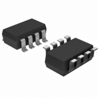
AD5171BRJ50-RL7 Analog Devices Inc, AD5171BRJ50-RL7 Datasheet - Page 13

AD5171BRJ50-RL7
Manufacturer Part Number
AD5171BRJ50-RL7
Description
IC DGTL POT OTP 50K SOT23-8
Manufacturer
Analog Devices Inc
Datasheet
1.AD5171BRJZ10-R7.pdf
(24 pages)
Specifications of AD5171BRJ50-RL7
Taps
64
Resistance (ohms)
50K
Number Of Circuits
1
Temperature Coefficient
35 ppm/°C Typical
Memory Type
Non-Volatile
Interface
I²C, 2-Wire Serial
Voltage - Supply
2.7 V ~ 5.5 V
Operating Temperature
-40°C ~ 125°C
Mounting Type
Surface Mount
Package / Case
SOT-23-8
Resistance In Ohms
50K
Number Of Elements
1
# Of Taps
64
Resistance (max)
50KOhm
Power Supply Requirement
Single
Interface Type
Serial (2-Wire/I2C)
Single Supply Voltage (typ)
3/5V
Dual Supply Voltage (typ)
Not RequiredV
Single Supply Voltage (min)
2.7V
Single Supply Voltage (max)
5.5V
Dual Supply Voltage (min)
Not RequiredV
Dual Supply Voltage (max)
Not RequiredV
Operating Temp Range
-40C to 125C
Operating Temperature Classification
Automotive
Mounting
Surface Mount
Pin Count
8
Lead Free Status / RoHS Status
Contains lead / RoHS non-compliant
For Use With
AD5171EVAL - BOARD EVAL FOR AD5171
Lead Free Status / RoHS Status
Not Compliant, Contains lead / RoHS non-compliant
VARIABLE RESISTANCE AND VOLTAGE FOR
RHEOSTAT MODE
If only the W-to-B or W-to-A terminals are used as variable
resistors, the unused terminal can be opened or shorted with
Terminal W. This operation is called rheostat mode (see Figure 26).
The nominal resistance (R
accessed by the wiper terminal, plus Terminal B contact if R
considered. The 6-bit data in the RDAC latch is decoded to
select one of the 64 settings. Assuming that a 10 kΩ part is used,
the first connection of the wiper starts at Terminal B for Data 0x00.
Such a connection yields a minimum of 60 Ω resistance between
Terminal W and Terminal B due to the 60 Ω wiper contact
resistance. The second connection is the first tap point, which
corresponds to 219 Ω (R
and so on. Each LSB data value increase moves the wiper up
the resistor ladder until the last tap point is reached at 10,060 Ω
(63 × R
equivalent RDAC circuit. The general equation determining R
where:
D is the decimal equivalent of the 6-bit binary code.
R
R
the internal switch.
Table 6. R
D (Dec)
63
32
1
0
Because a finite wiper resistance of 60 Ω is present in the zero-
scale condition, care should be taken to limit the current flow
between Terminal W and Terminal B in this state to a maximum
pulse current 20 mA. Otherwise, degradation or possible
destruction of the internal switch contact can occur.
AB
W
is the wiper resistance contributed by the on-resistance of
is the end-to-end resistance.
R
WB
AB
A
B
/63 + R
(
D
WB
)
=
vs. Codes: R
R
10060
5139
219
60
W
WB
Figure 26. Rheostat Mode Configuration
63
D
W
(Ω)
). Figure 27 shows a simplified diagram of the
×
R
AB
+
WB
A
B
Output State
Full-scale (R
Midscale
1 LSB
Zero-scale (wiper contact resistance)
AB
AB
R
= 1 × R
W
) of the RDAC has 64 contact points
= 10 kΩ; Terminal A Open
W
AB
/63 + R
AB
+ R
W
A
B
)
W
) for Data 0x01,
W
WB
WB
Rev. D | Page 13 of 24
(1)
is
is
Similar to the mechanical potentiometer, the resistance of the
RDAC between the wiper (Terminal W) and Terminal A also
produces a complementary resistance, R
are used, Terminal B can be opened or shorted to Terminal W.
Setting the resistance value for R
of resistance and decreases as the data loaded in the latch
increases in value. The general equation for this operation is
Table 7. R
D (Dec)
63
32
1
0
The typical distribution of the resistance tolerance from device
to device is process-lot dependent; it is possible to have ±30%
tolerance.
VARIABLE RESISTANCE AND VOLTAGE FOR
POTENTIOMETER MODE
If all three terminals are used, the operation is called the
potentiometer mode. The most common configuration is the
voltage divider operation (see Figure 28).
R
WA
(
D
WA
)
Figure 28. Potentiometer Mode Configuration
=
vs. Codes: R
Figure 27. AD5171 Equivalent RDAC Circuit
63
D5
D4
D3
D2
D1
D0
63
DECODER
−
R
60
4980
9901
10060
LATCH
RDAC
D
WA
AND
V
×
I
(Ω)
R
AB
AB
+
= 10 kΩ; Terminal B Open
A
B
R
R
R
R
W
S
S
S
W
WA
starts at a maximum value
Output State
Full-scale
Midscale
1 LSB
Zero-scale
WA
V
O
. When these terminals
A
W
B
AD5171
(2)


