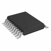
AD5428YRUZ Analog Devices Inc, AD5428YRUZ Datasheet - Page 6

AD5428YRUZ
Manufacturer Part Number
AD5428YRUZ
Description
IC DAC 8BIT DUAL MULT 20TSSOP
Manufacturer
Analog Devices Inc
Datasheet
1.AD5428YRUZ.pdf
(32 pages)
Specifications of AD5428YRUZ
Data Interface
Parallel
Settling Time
30ns
Number Of Bits
8
Number Of Converters
2
Voltage Supply Source
Single Supply
Power Dissipation (max)
3.3µW
Operating Temperature
-40°C ~ 125°C
Mounting Type
Surface Mount
Package / Case
20-TSSOP
Resolution (bits)
8bit
Sampling Rate
21.3MSPS
Input Channel Type
Parallel
Supply Voltage Range - Analogue
2.5V To 5.5V
Supply Current
500nA
Digital Ic Case Style
TSSOP
Package
20TSSOP
Resolution
8 Bit
Conversion Rate
21.3 MSPS
Architecture
R-2R
Digital Interface Type
Parallel
Number Of Outputs Per Chip
2
Output Type
Current
Full Scale Error
±25 mV
Integral Nonlinearity Error
±0.25 LSB
Maximum Settling Time
0.12 us
Lead Free Status / RoHS Status
Lead free / RoHS Compliant
For Use With
EVAL-AD5428EBZ - BOARD EVAL FOR AD5428
Lead Free Status / RoHS Status
Lead free / RoHS Compliant, Lead free / RoHS Compliant
Available stocks
Company
Part Number
Manufacturer
Quantity
Price
Part Number:
AD5428YRUZ
Manufacturer:
ADI/亚德诺
Quantity:
20 000
AD5428/AD5440/AD5447
ABSOLUTE MAXIMUM RATINGS
Transient currents of up to 100 mA do not cause SCR latch-up.
T
Table 3.
Parameter
V
V
I
Logic Inputs and Output
Operating Temperature Range
Storage Temperature Range
Junction Temperature
20-lead TSSOP θ
24-lead TSSOP θ
Lead Temperature, Soldering (10 sec)
IR Reflow, Peak Temperature (<20 sec)
1
ESD CAUTION
ESD (electrostatic discharge) sensitive device. Electrostatic charges as high as 4000 V readily accumulate on
the human body and test equipment and can discharge without detection. Although this product features
proprietary ESD protection circuitry, permanent damage may occur on devices subjected to high energy
electrostatic discharges. Therefore, proper ESD precautions are recommended to avoid performance
degradation or loss of functionality.
OUT
Overvoltages at DBx, CS , and R/ W are clamped by internal diodes.
DD
REF
A
Automotive (Y Version)
= 25°C, unless otherwise noted.
1, I
A, V
to GND
OUT
REF
2 to DGND
B, R
FB
A, R
JA
JA
Thermal Impedance
Thermal Impedance
FB
B to DGND
1
Rating
–0.3 V to +7 V
–12 V to +12 V
–0.3 V to +7 V
–0.3 V to V
–40°C to +125°C
–65°C to +150°C
150°C
143°C/W
128°C/W
300°C
235°C
DD
+ 0.3 V
Rev. B | Page 6 of 32
Stresses above those listed in Absolute Maximum Ratings may
cause permanent damage to the device. This is a stress rating
only; functional operation of the device at these or any other
conditions above those listed in the operational sections of this
specification is not implied. Exposure to absolute maximum
rating conditions for extended periods may affect device
reliability. Only one absolute maximum rating may be applied
at any one time.


