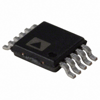
AD5624RBRMZ-5 Analog Devices Inc, AD5624RBRMZ-5 Datasheet

AD5624RBRMZ-5
Specifications of AD5624RBRMZ-5
Available stocks
Related parts for AD5624RBRMZ-5
AD5624RBRMZ-5 Summary of contents
Page 1
FEATURES Low power, quad nanoDACs AD5664: 16 bits AD5624: 12 bits Relative accuracy: ±12 LSBs max Guaranteed monotonic by design 10-lead MSOP and 3 mm × LFCSP_WD 2 5.5 V power supply Power-on reset to zero ...
Page 2
AD5624/AD5664 TABLE OF CONTENTS Features .............................................................................................. 1 Applications....................................................................................... 1 Functional Block Diagram .............................................................. 1 General Description ......................................................................... 1 Product Highlights ........................................................................... 1 Specifications..................................................................................... 3 AC Characteristics........................................................................ 4 Timing Characteristics ................................................................ 5 Timing Diagram ........................................................................... 5 Absolute Maximum Ratings............................................................ 6 ESD ...
Page 3
SPECIFICATIONS kΩ to GND Table 2. Parameter Min 2 STATIC PERFORMANCE AD5664 Resolution 16 Relative Accuracy Differential Nonlinearity AD5624 Resolution Relative Accuracy Differential Nonlinearity Zero-Code Error Offset ...
Page 4
AD5624/AD5664 Parameter Min POWER REQUIREMENTS V 2 (Normal Mode (All Power-Down DD 5 Modes 4 ...
Page 5
TIMING CHARACTERISTICS All input signals are specified with 2 5.5 V; all specifications T DD Table 4. Limit at T MIN 1 Parameter ...
Page 6
AD5624/AD5664 ABSOLUTE MAXIMUM RATINGS T = 25°C, unless otherwise noted. A Table 5. Parameter V to GND GND OUT V to GND REF Digital Input Voltage to GND Operating Temperature Range Industrial (A Grade, B Grade) Storage ...
Page 7
PIN CONFIGURATION AND FUNCTION DESCRIPTIONS Table 6. Pin Function Descriptions Pin No. Mnemonic Description Analog Output Voltage from DAC A. The output amplifier has rail-to-rail operation. OUT Analog Output Voltage from DAC B. The ...
Page 8
AD5624/AD5664 TYPICAL PERFORMANCE CHARACTERISTICS REF 25° –2 –4 –6 –8 – 10k 15k 20k 25k 30k 35k 40k 45k 50k 55k 60k 65k ...
Page 9
T = 25° –2 –4 –6 –8 2.7 3.2 3.7 4.2 4.7 V (V) DD Figure 10. INL and DNL Error vs. Supply –0.02 –0.04 GAIN ERROR –0.06 –0.08 ...
Page 10
AD5624/AD5664 3. 25° 0.39 0.40 0.41 I (mA) DD Figure 16. I Histogram with V DD 0.20 DAC LOADED WITH 5V, ...
Page 11
REF 2.537 T = 25°C A 2.536 5ns/SAMPLE NUMBER 2.535 GLITCH IMPULSE = 9.494nV 2.534 1LSB CHANGE AROUND MIDSCALE (0x8000 TO 0x7FFF) 2.533 2.532 2.531 2.530 2.529 2.528 2.527 2.526 2.525 2.524 2.523 ...
Page 12
AD5624/AD5664 5 0 –5 –10 –15 –20 –25 –30 –35 –40 10k 100k FREQUENCY (Hz) Figure 28. Multiplying Bandwidth 25° 10M Rev Page ...
Page 13
TERMINOLOGY Relative Accuracy or Integral Nonlinearity (INL) For the DAC, relative accuracy or integral nonlinearity is a measurement of the maximum deviation, in LSBs, from a straight line passing through the endpoints of the DAC transfer function. A typical INL ...
Page 14
AD5624/AD5664 Digital Crosstalk This is the glitch impulse transferred to the output of one DAC at midscale in response to a full-scale code change (all 0s to all 1s and vice versa) in the input register of another DAC. It ...
Page 15
THEORY OF OPERATION D/A SECTION The AD5624/AD5664 DACs are fabricated on a CMOS process. The architecture consists of a string DAC followed by an output buffer amplifier. Figure 29 shows a block diagram of the DAC architecture REF ...
Page 16
AD5624/AD5664 INPUT SHIFT REGISTER The input shift register is 24 bits wide The first two bits are don’t care bits. The next three bits are the Command bits (see Table 7), followed by the 3-bit DAC address, ...
Page 17
SOFTWARE RESET The AD5624/AD5664 contain a software reset function. Command 110 is reserved for the software reset function (see Table 7). The software reset command contains two reset modes that are software programmable by setting Bit DB0 in the control ...
Page 18
AD5624/AD5664 LDAC FUNCTION The AD5624/AD5664 DACs have double-buffered interfaces consisting of two banks of registers: input registers and DAC registers. The input registers are connected directly to the input shift register and the digital code is transferred to the relevant ...
Page 19
MICROPROCESSOR INTERFACING AD5624/AD5664 to Blackfin® ADSP-BF53x Interface Figure 35 shows a serial interface between the AD5624/AD5664 and the Blackfin ADSP-BF53x microprocessor. The ADSP-BF53x processor family incorporates two dual-channel synchronous serial ports, SPORT1 and SPORT0, for serial and multiprocessor commu- nications. ...
Page 20
AD5624/AD5664 APPLICATIONS CHOOSING A REFERENCE FOR THE AD5624/AD5664 To achieve the optimum performance from the AD5624/ AD5664, thought should be given to the choice of a precision voltage reference. The AD5624/AD5664 have only one reference input The voltage ...
Page 21
BIPOLAR OPERATION USING THE AD5624/AD5664 The AD5624/AD5664 have been designed for single-supply operation, but a bipolar output range is also possible using the circuit in Figure 40. The circuit gives an output voltage range of ±5 V. Rail-to-rail operation at ...
Page 22
AD5624/AD5664 OUTLINE DIMENSIONS ORDERING GUIDE Model Temperature Range AD5624BRMZ −40°C to +105°C AD5624BRMZ-REEL7 −40°C to +105°C AD5624BCPZ-250RL7 −40°C to +105°C AD5624BCPZ-REEL7 −40°C to +105°C AD5664ARMZ −40°C to +105°C AD5664ARMZ-REEL7 −40°C to +105°C AD5664BRMZ −40°C to +105°C AD5664BRMZ-REEL7 −40°C to +105°C ...
Page 23
NOTES Rev Page AD5624/AD5664 ...
Page 24
AD5624/AD5664 NOTES ©2006 Analog Devices, Inc. All rights reserved. Trademarks and registered trademarks are the property of their respective owners. D05943-0-6/06(0) Rev Page ...


