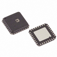
AD9744ACPZ Analog Devices Inc, AD9744ACPZ Datasheet - Page 18

AD9744ACPZ
Manufacturer Part Number
AD9744ACPZ
Description
IC DAC 14BIT 210MSPS 32-LFCSP
Manufacturer
Analog Devices Inc
Series
TxDAC®r
Datasheet
1.AD9744ARUZ.pdf
(32 pages)
Specifications of AD9744ACPZ
Data Interface
Parallel
Settling Time
11ns
Number Of Bits
14
Number Of Converters
1
Voltage Supply Source
Analog and Digital
Power Dissipation (max)
145mW
Operating Temperature
-40°C ~ 85°C
Mounting Type
Surface Mount
Package / Case
32-LFCSP
Resolution (bits)
14bit
Sampling Rate
210MSPS
Input Channel Type
Parallel
Supply Voltage Range - Analog
2.7V To 3.6V
Supply Voltage Range - Digital
2.7V To 3.6V
Number Of Channels
1
Resolution
14b
Interface Type
Parallel
Single Supply Voltage (typ)
3.3V
Dual Supply Voltage (typ)
Not RequiredV
Power Supply Requirement
Analog and Digital
Output Type
Current
Integral Nonlinearity Error
±5LSB
Single Supply Voltage (min)
2.7V
Single Supply Voltage (max)
3.6V
Dual Supply Voltage (min)
Not RequiredV
Dual Supply Voltage (max)
Not RequiredV
Operating Temp Range
-40C to 85C
Operating Temperature Classification
Industrial
Mounting
Surface Mount
Pin Count
32
Package Type
LFCSP EP
Lead Free Status / RoHS Status
Lead free / RoHS Compliant
For Use With
AD9744ACP-PCBZ - BOARD EVAL FOR AD9744ACP
Lead Free Status / Rohs Status
Compliant
Available stocks
Company
Part Number
Manufacturer
Quantity
Price
Part Number:
AD9744ACPZ
Manufacturer:
ADI/亚德诺
Quantity:
20 000
Company:
Part Number:
AD9744ACPZRL7
Manufacturer:
AD
Quantity:
1 400
Part Number:
AD9744ACPZRL7
Manufacturer:
ADI/亚德诺
Quantity:
20 000
AD9744
capabilities should all be considered when optimizing this
circuit.
The differential circuit shown in Figure 36 provides the neces-
sary level shifting required in a single-supply system. In this
case, AVDD, which is the positive analog supply for both the
AD9744 and the op amp, is also used to level-shift the differen-
tial output of the AD9744 to midsupply (that is, AVDD/2). The
AD8041 is a suitable op amp for this application.
SINGLE-ENDED UNBUFFERED VOLTAGE OUTPUT
Figure 37 shows the AD9744 configured to provide a unipolar
output range of approximately 0 V to 0.5 V for a doubly termi-
nated 50 Ω cable since the nominal full-scale current, I
20 mA flows through the equivalent R
R
or IOUTB. The unused output (IOUTA or IOUTB) can be con-
nected to ACOM directly or via a matching R
values of I
compliance range is adhered to. One additional consideration
in this mode is the integral nonlinearity (INL), discussed in
the Analog Outputs section. For optimum INL performance,
the single-ended, buffered voltage output configuration is
suggested.
SINGLE-ENDED, BUFFERED VOLTAGE OUTPUT
CONFIGURATION
Figure 38 shows a buffered single-ended output configuration
in which the op amp U1 performs an I-V conversion on the
AD9744 output current. U1 maintains IOUTA (or IOUTB) at a
virtual ground, minimizing the nonlinear output impedance
effect on the DAC’s INL performance as described in the
Analog Outputs section. Although this single-ended configura-
tion typically provides the best dc linearity performance, its ac
distortion performance at higher DAC update rates may be
limited by U1’s slew rate capabilities. U1 provides a negative
unipolar output voltage, and its full-scale output voltage is sim-
ply the product of R
LOAD
AD9744
represents the equivalent load resistance seen by IOUTA
AD9744
IOUTA
IOUTB
Figure 36. Single-Supply DC Differential Coupled Circuit
OUTFS
IOUTA
IOUTB
Figure 37. 0 V to 0.5 V Unbuffered Voltage Output
22
21
and R
25Ω
22
21
I
OUTFS
FB
LOAD
C
and I
OPT
25Ω
= 20mA
can be selected as long as the positive
OUTFS
25Ω
225Ω
225Ω
. The full-scale output should be
50Ω
LOAD
1kΩ
of 25 Ω. In this case,
AD8041
V
500Ω
OUTA
LOAD
50Ω
1kΩ
= 0V TO 0.5V
. Different
OUTFS
AVDD
, of
Rev. B | Page 18 of 32
set within U1’s voltage output swing capabilities by scaling I
and/or R
result with a reduced I
required to sink less signal current.
POWER AND GROUNDING CONSIDERATIONS,
POWER SUPPLY REJECTION
Many applications seek high speed and high performance
under less than ideal operating conditions. In these application
circuits, the implementation and construction of the printed
circuit board is as important as the circuit design. Proper RF
techniques must be used for device selection, placement, and
routing as well as power supply bypassing and grounding to
ensure optimum performance. Figure 43 to Figure 46 illustrate
the recommended printed circuit board ground, power, and signal
plane layouts implemented on the AD9744 evaluation board.
One factor that can measurably affect system performance is
the ability of the DAC output to reject dc variations or ac noise
superimposed on the analog or digital dc power distribution.
This is referred to as the power supply rejection ratio (PSRR).
For dc variations of the power supply, the resulting performance
of the DAC directly corresponds to a gain error associated with
the DAC’s full-scale current, I
is common in applications where the power distribution is gen-
erated by a switching power supply. Typically, switching power
supply noise will occur over the spectrum from tens of kHz to
several MHz. The PSRR vs. frequency of the AD9744 AVDD
supply over this frequency range is shown in Figure 39.
AD9744
85
80
75
70
65
60
55
50
45
40
IOUTA
IOUTB
Figure 39. Power Supply Rejection Ratio (PSRR) vs. Frequency
0
FB
. An improvement in ac distortion performance may
22
21
Figure 38. Unipolar Buffered Voltage Output
2
I
OUTFS
OUTFS
= 10mA
4
FREQUENCY (MHz)
200Ω
since the signal current U1 will be
OUTFS
6
. AC noise on the dc supplies
200Ω
C
R
U1
OPT
FB
8
V
10
OUT
= I
OUTFS
12
× R
OUTFS
FB


