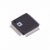
ADV7123JSTZ330 Analog Devices Inc, ADV7123JSTZ330 Datasheet - Page 6

ADV7123JSTZ330
Manufacturer Part Number
ADV7123JSTZ330
Description
IC DAC VIDEO 3CH 330MHZ 48-LQFP
Manufacturer
Analog Devices Inc
Datasheet
1.ADV7123KSTZ50.pdf
(24 pages)
Specifications of ADV7123JSTZ330
Data Interface
Parallel
Settling Time
15ns
Number Of Bits
10
Number Of Converters
3
Voltage Supply Source
Single Supply
Power Dissipation (max)
30mW
Operating Temperature
0°C ~ 70°C
Mounting Type
Surface Mount
Package / Case
48-LQFP
Resolution (bits)
10bit
Sampling Rate
330MSPS
Input Channel Type
Parallel
Supply Current
16mA
Digital Ic Case Style
QFP
No. Of Pins
48
Lead Free Status / RoHS Status
Lead free / RoHS Compliant
Available stocks
Company
Part Number
Manufacturer
Quantity
Price
Company:
Part Number:
ADV7123JSTZ330
Manufacturer:
TOSHIBA
Quantity:
6 219
Company:
Part Number:
ADV7123JSTZ330
Manufacturer:
ADI
Quantity:
210
Company:
Part Number:
ADV7123JSTZ330
Manufacturer:
Analog Devices Inc
Quantity:
10 000
Part Number:
ADV7123JSTZ330
Manufacturer:
ADI/亚德诺
Quantity:
20 000
ADV7123
Parameter
DAC PERFORMANCE
1
2
3
4
5
3.3 V DYNAMIC SPECIFICATIONS
V
Table 4.
Parameter
AC LINEARITY
These maximum/minimum specifications are guaranteed by characterization over the 4.75 V to 5.25 V range.
Note that the ADV7123 exhibits high performance when operating with an internal voltage reference, V
DAC-to-DAC crosstalk is measured by holding one DAC high while the other two are making low-to-high and high-to-low transitions.
Clock and data feedthrough is a function of the amount of overshoot and undershoot on the digital inputs. Glitch impulse includes clock and data feedthrough.
TTL input values are 0 V to 3 V, with input rise/fall times of −3 ns, measured from the 10% and 90% points. Timing reference points are 50% for inputs and outputs.
AA
Glitch Impulse
DAC-to-DAC Crosstalk
Data Feedthrough
Clock Feedthrough
Spurious-Free Dynamic Range to Nyquist
Spurious-Free Dynamic Range Within a Window
= 3.0 V to 3.6 V
Single-Ended Output
Double-Ended Output
Single-Ended Output
Double-Ended Output
f
f
f
f
f
f
f
f
f
f
f
f
f
f
f
f
f
f
f
f
f
f
f
f
f
f
f
f
f
f
CLK
CLK
CLK
CLK
CLK
CLK
CLK
CLK
CLK
CLK
CLK
CLK
CLK
CLK
CLK
CLK
CLK
CLK
CLK
CLK
CLK
CLK
CLK
CLK
CLK
CLK
CLK
CLK
CLK
CLK
= 50 MHz; f
= 50 MHz; f
= 50 MHz; f
= 50 MHz; f
= 100 MHz; f
= 100 MHz; f
= 100 MHz; f
= 100 MHz; f
= 140 MHz; f
= 140 MHz; f
= 140 MHz; f
= 140 MHz; f
= 50 MHz; f
= 50 MHz; f
= 50 MHz; f
= 50 MHz; f
= 100 MHz; f
= 100 MHz; f
= 100 MHz; f
= 100 MHz; f
= 140 MHz; f
= 140 MHz; f
= 140 MHz; f
= 140 MHz; f
= 50 MHz; f
= 50 MHz; f
= 140 MHz; f
= 50 MHz; f
= 50 MHz; f
= 140 MHz; f
1
1
4, 5
, V
4, 5
OUT
OUT
OUT
OUT
OUT
OUT
OUT
OUT
OUT
OUT
OUT
OUT
OUT
OUT
OUT
OUT
OUT
OUT
OUT
OUT
OUT
OUT
OUT
OUT
OUT
OUT
OUT
OUT
OUT
OUT
REF
3
= 1.00 MHz
= 2.51 MHz
= 5.04 MHz
= 20.2 MHz
= 1.00 MHz
= 2.51 MHz
= 5.04 MHz
= 20.2 MHz
= 1.00 MHz; 1 MHz Span
= 5.04 MHz; 2 MHz Span
= 1.00 MHz; 1 MHz Span
= 5.00 MHz; 2 MHz Span
= 2.51 MHz
= 5.04 MHz
= 20.2 MHz
= 40.4 MHz
= 2.51 MHz
= 5.04 MHz
= 20.2 MHz
= 40.4 MHz
= 2.51 MHz
= 5.04 MHz
= 20.2 MHz
= 40.4 MHz
= 2.51 MHz
= 5.04 MHz
= 20.2 MHz
= 40.4 MHz
= 5.04 MHz; 4 MHz Span
= 5.00 MHz; 4 MHz Span
= 1.235 V, R
SET
= 680 Ω, C
2
L
= 10 pF. All specifications are T
Rev. D | Page 6 of 24
A
REF
= 25°C, unless otherwise noted, T
.
Min
Min
Typ
67
67
63
55
62
60
54
48
57
58
52
41
70
70
65
54
67
63
58
52
62
61
55
53
77
73
64
74
73
60
23
22
33
Typ
10
Max
Max
J MAX
= 110°C.
Unit
dBc
dBc
dBc
dBc
dBc
dBc
dBc
dBc
dBc
dBc
dBc
dBc
dBc
dBc
dBc
dBc
dBc
dBc
dBc
dBc
dBc
dBc
dBc
dBc
dBc
dBc
dBc
dBc
dBc
dBc
Unit
pV-sec
dB
dB
dB


