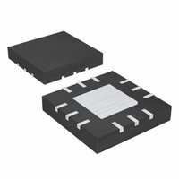
MAX5531ETC+ Maxim Integrated Products, MAX5531ETC+ Datasheet - Page 16

MAX5531ETC+
Manufacturer Part Number
MAX5531ETC+
Description
IC DAC 12BIT SGL ULP 12-TQFN
Manufacturer
Maxim Integrated Products
Datasheet
1.MAX5531ETC.pdf
(19 pages)
Specifications of MAX5531ETC+
Settling Time
660µs
Number Of Bits
12
Data Interface
MICROWIRE™, QSPI™, Serial, SPI™
Number Of Converters
1
Voltage Supply Source
Single Supply
Power Dissipation (max)
1.35mW
Operating Temperature
-40°C ~ 85°C
Mounting Type
Surface Mount
Package / Case
12-TQFN Exposed Pad
Number Of Dac Outputs
1
Resolution
12 bit
Interface Type
Serial (SPI)
Supply Voltage (max)
5.5 V
Supply Voltage (min)
1.8 V
Maximum Operating Temperature
+ 85 C
Mounting Style
SMD/SMT
Minimum Operating Temperature
- 40 C
Supply Current
0.007 mA
Voltage Reference
Internal
Lead Free Status / RoHS Status
Lead free / RoHS Compliant
See Figure 3 for an illustration of how to power the
MAX5530/MAX5531 with either one lithium-ion battery
or two alkaline batteries. The low current consumption
of the devices makes the MAX5530/MAX5531 ideal for
battery-powered applications.
See the circuit in Figure 4 for an illustration of how to
configure the MAX5530 as a programmable current
source for driving an LED. The MAX5530 drives a stan-
dard NPN transistor to program the current source. The
current source (I
Figure 4.
See the circuit in Figure 5 for an illustration of how to con-
figure the MAX5530 to bias a current output transducer.
In Figure 5, the output voltage of the MAX5530 is a func-
tion of the voltage drop across the transducer added to
the voltage drop across the feedback resistor R.
See the circuit in Figure 6 for an illustration of how to
use the MAX5531 to bias a two-electrode potentiostat
on the input of an ADC.
Figure 7 shows the MAX5530 in a unipolar output con-
figuration with unity gain. Table 4 lists the unipolar out-
put codes.
Ultra-Low-Power, 12-Bit,
Voltage-Output DACs
Figure 3. Portable Application Using Two Alkaline Cells or One Lithium Coin Cell
16
______________________________________________________________________________________
Voltage Biasing a Current-Output
Applications Information
Programmable Current Source
LED
0.1µF
Self-Biased Two-Electrode
) is defined in the equation in
Potentiostat Application
1-Cell and 2-Cell Circuit
1.8V ≤ V
2.2V ≤ V
ALKALINE
LITHIUM
REFERENCE)
Unipolar Output
(1µA, 1.25V
MAX6006
SHUNT
≤ 3.3V
≤ 3.3V
Transducer
536kΩ
+1.25V
0.01µF
REFIN
The MAX5530 output can be configured for bipolar
operation, as shown in Figure 8. The output voltage is
given by the following equation:
where N
binary input code. Table 5 shows digital codes (offset
binary) and the corresponding output voltage for the
circuit in Figure 4.
The MAX5530/MAX5531 have a force-sense output,
which provides a connection directly to the inverting ter-
minal of the output op amp, yielding the most flexibility.
The advantage of the force-sense output is that specific
gains can be set externally for a given application. The
gain error for the MAX5530/MAX5531 is specified in a
unity-gain configuration (op-amp output and inverting ter-
minals connected), and additional gain error results from
external resistor tolerances. Another advantage of the
force-sense DAC is that it allows many useful circuits to
be created with only a few simple external components.
An example of a custom fixed gain using the force-sense
output of the MAX5530/MAX5531 is shown in Figure 9. In
this example, R1 and R2 set the gain for V
where N
input code.
MAX5530
DAC
V
OUT
A
A
V
GND
V
DD
=[(V
represents the numeric value of the DAC’s
represents the numeric value of the DAC
OUT
REFIN
= V
REF
x N
Configurable Output Gain
x [(N
A
) / 4096] x [1 + (R2 / R1)]
VOUT
N
OF THE DAC INPUT CODE.
V
OUT
DAC
A
=
IS THE NUMERIC VALUE
- 2048) / 2048]
V
V
REFIN
OUT
4096
(0.30mV / LSB)
× N
Bipolar Output
DAC
OUT
.


