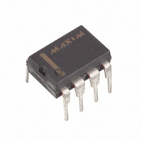
MAX517BCPA+ Maxim Integrated Products, MAX517BCPA+ Datasheet - Page 14

MAX517BCPA+
Manufacturer Part Number
MAX517BCPA+
Description
IC DAC 2-WIRE SRL 8BIT R-R 8-DIP
Manufacturer
Maxim Integrated Products
Datasheet
1.MAX518BCPA.pdf
(16 pages)
Specifications of MAX517BCPA+
Settling Time
6µs
Number Of Bits
8
Data Interface
I²C, Serial
Number Of Converters
2
Voltage Supply Source
Single Supply
Power Dissipation (max)
842mW
Operating Temperature
0°C ~ 70°C
Mounting Type
Through Hole
Package / Case
8-DIP (0.300", 7.62mm)
Number Of Dac Outputs
1
Resolution
8 bit
Interface Type
Serial (I2C)
Supply Voltage (max)
5.5 V
Supply Voltage (min)
4.5 V
Maximum Operating Temperature
+ 70 C
Mounting Style
Through Hole
Maximum Power Dissipation
727 mW
Minimum Operating Temperature
0 C
Supply Current
1.5 mA
Voltage Reference
External
Lead Free Status / RoHS Status
Lead free / RoHS Compliant
Bypass V
V
minimizes crosstalk among DAC outputs, reference
inputs, and digital inputs. Figure 16 shows the suggest-
ed PC board layout to minimize crosstalk.
When using the MAX518 (or the MAX517/MAX519 with
V
ter to the V
input(s) (Figure 18), especially in noisy environments.
The reference input’s bandwidth exceeds 1MHz for AC
signals, so disturbances on the reference input can
easily affect the DAC output(s).
The maximum input current for a single reference input
is V
that changes in the reference input current will have lit-
tle effect on the reference voltage. For example, with R
= 6Ω, the maximum output error due to R
In Figure 18, there is a voltage drop across R
adds to the TUE. This voltage drop is due to the sum of
the reference input current (V
ply current (6mA maximum), and the amplifier output
current (V
drop to an acceptable value. For example, with a 10kΩ
load, you can limit the error due to R
(9.8mV) by selecting R
2-Wire Serial 8-Bit DACs with
Rail-to-Rail Outputs
Figure 16. PC Board Layout for Minimizing MAX519 Crosstalk
(bottom view)
14
__________Applications Information
DD
DD
REF
as the reference), you may want to add a noise fil-
______________________________________________________________________________________
and GND as possible. Careful PC board layout
/16kΩ = I
OUT1
REF0
REF1
N.C.
DD
6Ω x I
R
R
REF
F
F
DD
with a 0.1µF capacitor, located as close to
= V
≤ 1.4Ω
/R
5V / 10kΩ)
supply (Figure 17) or to the reference
REF
LOAD
R F
REF
Power-Supply Bypassing and
/ I
(max) = 1.9mV or 0.1LSB
(max). In Figure 17, choose R
). Choose R
R F
F
SYSTEM GND
so that:
≤ 9.8mV / (5V / 16kΩ + 6mA +
Ground Management
REF
/16kΩ maximum), sup-
F
to limit this voltage
F
is given by:
F
OUT0
N.C.
N.C.
GND
to 0.5LSB
F
F
that
so
F
Figure 17. Reference Filter When Using V
Figure 18. V
+5V
+5V
DD
C
R
R
C
Filter When Using V
F
F
F
F
REF_
MAX518
MAX517
MAX519
V
V
DD
DD
DD
as a Reference
DD
0.1µF
as a Reference
0.1µF


