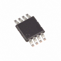
MAX5533EUA+ Maxim Integrated Products, MAX5533EUA+ Datasheet

MAX5533EUA+
Specifications of MAX5533EUA+
Related parts for MAX5533EUA+
MAX5533EUA+ Summary of contents
Page 1
... Programmable LCD Bias SPI and QSPI are trademarks of Motorola, Inc. MICROWIRE is a trademark of National Semiconductor Corp. µMAX is a registered trademark of Maxim Integrated Products, Inc. ________________________________________________________________ Maxim Integrated Products For pricing, delivery, and ordering information, please contact Maxim/Dallas Direct! at 1-888-629-4642, or visit Maxim’s website at www.maxim-ic.com. ...
Page 2
Dual, Ultra-Low-Power, 12-Bit, Voltage-Output DACs ABSOLUTE MAXIMUM RATINGS V to GND ..............................................................-0.3V to +6V DD OUTA, OUTB to GND .................................-0. FBA, FBB to GND .......................................-0. SCLK, DIN GND ..............................-0. REFIN, REFOUT to ...
Page 3
ELECTRICAL CHARACTERISTICS (continued +1.8V to +5.5V, OUT_ unloaded PARAMETER SYMBOL Gain-Error Temperature Coefficient Power-Supply Rejection Ratio REFERENCE INPUT (MAX5532/MAX5534) Reference-Input Voltage Range V Reference-Input Impedance R REFERENCE OUTPUT (MAX5533/MAX5535) Initial Accuracy V Output-Voltage Temperature V TEMPCO ...
Page 4
Dual, Ultra-Low-Power, 12-Bit, Voltage-Output DACs ELECTRICAL CHARACTERISTICS (continued +1.8V to +5.5V, OUT_ unloaded PARAMETER SYMBOL DAC OUTPUTS (OUTA, OUTB) Capacitive Driving Capability Short-Circuit Current (Note 6) DAC Power-Up Time Output Power-Up Glitch FB_ Input Current DIGITAL ...
Page 5
ELECTRICAL CHARACTERISTICS (continued +1.8V to +5.5V, OUT_ unloaded PARAMETER SYMBOL POWER REQUIREMENTS Supply Voltage Range Supply Current (Note 9) Standby Supply Current Shutdown Supply Current TIMING CHARACTERISTICS (V = +4.5V to +5.5V ...
Page 6
Dual, Ultra-Low-Power, 12-Bit, Voltage-Output DACs TIMING CHARACTERISTICS ( +1.8V to +5.5V MIN to T MAX , unless otherwise noted. Typical values are +25 C.) PARAMETER TIMING CHARACTERISTICS (V = 1.8V ...
Page 7
V = 4.096V (MAX5532/MAX5534 REF SUPPLY CURRENT vs. SUPPLY VOLTAGE (MAX5532/MAX5534) 5.0 4.5 4.0 3.5 3.0 2.5 2.0 1.5 1.0 0.5 0 1.5 2.0 2.5 3.0 3.5 4.0 4.5 5.0 5.5 SUPPLY VOLTAGE (V) SUPPLY ...
Page 8
Dual, Ultra-Low-Power, 12-Bit, Voltage-Output DACs (V = 5.0V 4.096V (MAX5532/MAX5534 REF INL vs. INPUT CODE ( 1.8V) DD REF 500 1000 1500 2000 2500 ...
Page 9
V = 4.096V (MAX5532/MAX5534 REF DAC OUTPUT VOLTAGE vs. OUTPUT SOURCE CURRENT REF DD CODE = MIDSCALE ...
Page 10
Dual, Ultra-Low-Power, 12-Bit, Voltage-Output DACs (V = 5.0V 4.096V (MAX5532/MAX5534 REF REFERENCE OUTPUT VOLTAGE vs. REFERENCE OUTPUT CURRENT 3. 3.91 3.90 3.89 3.88 -500 2000 4500 7000 9500 12,000 14,500 REFERENCE OUTPUT ...
Page 11
V = 4.096V (MAX5532/MAX5534 REF REFERENCE LOAD TRANSIENT (V = 5V) DD 200 s/div REFERENCE PSRR vs. FREQUENCY 0.01 0.1 1 FREQUENCY ...
Page 12
Dual, Ultra-Low-Power, 12-Bit, Voltage-Output DACs PIN MAX5532 MAX5533 MAX5534 — 4 — 4 — — — — — ...
Page 13
Voltage-Output DACs V DD POWER- 2-BIT DOWN PROGRAMMABLE CONTROL REFERENCE INPUT REGISTER CONTROL SCLK LOGIC DIN AND SHIFT CS REGISTER INPUT REGISTER GND V DD POWER- DOWN MAX5534 CONTROL INPUT REGISTER CONTROL SCLK LOGIC DIN AND SHIFT CS REGISTER ...
Page 14
Dual, Ultra-Low-Power, 12-Bit, Voltage-Output DACs POWER- DOWN CONTROL CONTROL SCLK LOGIC DIN AND SHIFT CS REGISTER Detailed Description The MAX5532–MAX5535 dual, 12-bit, ultra-low-power, voltage-output DACs offer rail-to-rail buffered voltage outputs. The DACs operate from a 1.8V to 5.5V supply and ...
Page 15
Table 1. Serial Write Data Format CONTROL MSB D11 SCLK DIN CSW Figure 1. Timing Diagram SCLK DIN CONTROL BITS CS Figure 2. Register Loading Diagram ...
Page 16
Dual, Ultra-Low-Power, 12-Bit, Voltage-Output DACs Table 2. Serial-Interface Programming Commands CONTROL BITS INPUT DATA D11– XXXXXXXXXXXX 12-bit data 12–bit data ...
Page 17
The MAX5532–MAX5535 feature two power modes to conserve power during idle periods. In normal opera- tion, the device is fully operational. In shutdown mode, the device is completely powered down, including the internal voltage reference in the MAX5533/MAX5535. The MAX5533/MAX5535 ...
Page 18
Dual, Ultra-Low-Power, 12-Bit, Voltage-Output DACs Applications Information 1-Cell and 2-Cell Circuits See Figure 3 for an illustration of how to power the MAX5532–MAX5535 with either one lithium-ion battery or two alkaline batteries. The low current consumption of the devices make ...
Page 19
Voltage Biasing a Current-Output Transducer See the circuit in Figure 5 for an illustration of how to configure the MAX5534/MAX5535 to bias a current-out- put transducer. In Figure 5, the output voltage of the MAX5534/MAX5535 is a function of the ...
Page 20
Dual, Ultra-Low-Power, 12-Bit, Voltage-Output DACs 10k DAC REFIN 1/2 MAX5534 Figure 7. Bipolar Output Circuit REFIN DAC VOUTA R2 FBA MAX5534 R1 DAC VOUTB FBB Figure 8. Separate Force-Sense Outputs Create Unity and Greater-than-Unity DAC Gains Using the Same Reference ...
Page 21
REF OUTA DAC FBA MAX5535 REF OUTB DAC FBB REFOUT BAND GAP Figure 11. Driven Two-Electrode Potentiostat Application ______________________________________________________________________________________ Dual, Ultra-Low-Power, 12-Bit, Voltage-Output DACs Pin Configurations (continued) TOP VIEW TO ADC SENSOR CE TO ADC ...
Page 22
Dual, Ultra-Low-Power, 12-Bit, Voltage-Output DACs (The package drawing(s) in this data sheet may not reflect the most current specifications. For the latest package outline information www.maxim-ic.com/packages.) 22 ______________________________________________________________________________________ Package Information PACKAGE OUTLINE, 12, 16, 20, 24, 28L THIN ...
Page 23
For the latest package outline information www.maxim-ic.com/packages.) ______________________________________________________________________________________ Dual, Ultra-Low-Power, 12-Bit, Voltage-Output DACs Package Information (continued) PACKAGE OUTLINE, 12, 16, 20, 24, 28L THIN ...
Page 24
... Maxim cannot assume responsibility for use of any circuitry other than circuitry entirely embodied in a Maxim product. No circuit patent licenses are implied. Maxim reserves the right to change the circuitry and specifications without notice at any time. 24 ____________________Maxim Integrated Products, 120 San Gabriel Drive, Sunnyvale, CA 94086 408-737-7600 © 2007 Maxim Integrated Products ...


