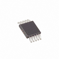
MAX5842LEUB+ Maxim Integrated Products, MAX5842LEUB+ Datasheet

MAX5842LEUB+
Specifications of MAX5842LEUB+
Related parts for MAX5842LEUB+
MAX5842LEUB+ Summary of contents
Page 1
... GND 4 SDA 5 µMAX Rail-to-Rail is a registered trademark of Nippon Motorola, Ltd trademark of Philips Corp. ________________________________________________________________ Maxim Integrated Products For pricing, delivery, and ordering information, please contact Maxim/Dallas Direct! at 1-888-629-4642, or visit Maxim’s website at www.maxim-ic.com. Voltage-Output DAC o Ultra-Low Supply Current 2 C ™ -compatible, 230µ ...
Page 2
Quad, 12-Bit, Low-Power, 2-Wire, Serial Voltage-Output DAC ABSOLUTE MAXIMUM RATINGS V , SCL, SDA to GND ............................................-0.3V to +6V DD OUT_, REF, ADD to GND..............................-0. Maximum Current into Any Pin............................................50mA Continuous Power Dissipation (T = +70°C) A 10-Pin ...
Page 3
Quad, 12-Bit, Low-Power, 2-Wire, Serial ELECTRICAL CHARACTERISTICS (continued +2.7V to +5.5V, GND = REF +5V +25°C.) (Note PARAMETER SYMBOL Input Hysteresis Input Leakage Current Input Capacitance DIGITAL ...
Page 4
Quad, 12-Bit, Low-Power, 2-Wire, Serial Voltage-Output DAC ELECTRICAL CHARACTERISTICS (continued +2.7V to +5.5V, GND = REF +5V +25°C.) (Note PARAMETER SYMBOL Bus Capacitance Maximum Duration ...
Page 5
Quad, 12-Bit, Low-Power, 2-Wire, Serial (V = +5V 5kΩ.) DD L ZERO-CODE ERROR vs. SUPPLY VOLTAGE LOAD 0 2.7 3.4 4.1 4.8 SUPPLY VOLTAGE (V) GAIN ERROR vs. TEMPERATURE -2.0 -1.6 -1.2 ...
Page 6
Quad, 12-Bit, Low-Power, 2-Wire, Serial Voltage-Output DAC (V = +5V 5kΩ.) DD L POWER-DOWN SUPPLY CURRENT vs. SUPPLY VOLTAGE 500 Z = HIGH IMPEDANCE OUT NO LOAD 400 300 T = -40° +25°C A 200 ...
Page 7
Quad, 12-Bit, Low-Power, 2-Wire, Serial (V = +5V 5kΩ.) DD L SETTLING TIME (NEGATIVE) OUT_ C LOAD CODE = C00 hex TO 400 hex 2µs/div Note 6: The ability to drive loads less than 5kΩ is not implied. ...
Page 8
Quad, 12-Bit, Low-Power, 2-Wire, Serial Voltage-Output DAC PIN NAME 1 ADD Address Select. A logic high sets the address LSB logic low sets the address LSB to zero. 2 SCL Serial Clock Input 3 V Power Supply ...
Page 9
Quad, 12-Bit, Low-Power, 2-Wire, Serial Table 1. Power-Down Command Bits POWER-DOWN COMMAND BITS MODE/FUNCTION PD1 PD0 Power-up device. DAC output 0 0 restored to previous value. Power-down mode 0. Power down 0 1 device with output floating. Power-down mode 1. ...
Page 10
Quad, 12-Bit, Low-Power, 2-Wire, Serial Voltage-Output DAC SCL SDA Figure 2. START and STOP Conditions SCL SDA STOP START LEGAL STOP CONDITION SCL SDA START ILLEGAL STOP ILLEGAL EARLY STOP CONDITION Figure 3. Early STOP Conditions read ...
Page 11
Quad, 12-Bit, Low-Power, 2-Wire, Serial MSB MSB D7 D6 MSB MSB X X Figure 6. Example Write Command Sequences to the selected power-down mode based on the states of PD0 and PD1 ...
Page 12
Quad, 12-Bit, Low-Power, 2-Wire, Serial Voltage-Output DAC Table 3. Command Byte Definitions SERIAL DATA INPUT D11 DAC DATA DAC DATA DAC DATA DAC 0 ...
Page 13
Quad, 12-Bit, Low-Power, 2-Wire, Serial Table 3. Command Byte Definitions (continued) SERIAL DATA INPUT D11 ...
Page 14
Quad, 12-Bit, Low-Power, 2-Wire, Serial Voltage-Output DAC INPUT REGISTER A INPUT REGISTER B INPUT REGISTER C INPUT REGISTER D SERIAL INTERFACE SDA ADD SCL 14 ______________________________________________________________________________________ REF 12-BIT MUX AND DAC DAC REGISTER A 12-BIT MUX AND DAC DAC REGISTER ...
Page 15
... Maxim cannot assume responsibility for use of any circuitry other than circuitry entirely embodied in a Maxim product. No circuit patent licenses are implied. Maxim reserves the right to change the circuitry and specifications without notice at any time. Maxim Integrated Products, 120 San Gabriel Drive, Sunnyvale, CA 94086 408-737-7600 ____________________ 15 © 2002 Maxim Integrated Products ...


