MAX5722EUA+ Maxim Integrated Products, MAX5722EUA+ Datasheet
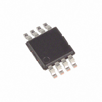
IC DAC 12BIT DUAL LP SER 8-UMAX

MAX5722EUA+

Manufacturer Part Number
MAX5722EUA+
Description
IC DAC 12BIT DUAL LP SER 8-UMAX
Manufacturer
Maxim Integrated Products
Datasheet

Specifications of MAX5722EUA+

Settling Time
4µs
Number Of Bits
12
Data Interface
Serial
Number Of Converters
2
Voltage Supply Source
Single Supply
Operating Temperature
-40°C ~ 85°C
Mounting Type
Surface Mount
Package / Case
8-MSOP, Micro8™, 8-uMAX, 8-uSOP,
Resolution
10 bit
Interface Type
Serial (SPI)
Supply Voltage (max)
5.5 V
Supply Voltage (min)
2.7 V
Maximum Operating Temperature
+ 85 C
Mounting Style
SMD/SMT
Minimum Operating Temperature
- 40 C
Supply Current
0.215 mA
Voltage Reference
External
Lead Free Status / RoHS Status
Lead free / RoHS Compliant
Power Dissipation (max)
-
Lead Free Status / Rohs Status
Lead free / RoHS Compliant
The MAX5722 dual,12-bit, low-power, buffered voltage-
output, digital-to-analog converter (DAC) is packaged
in a space-saving 8-pin µMAX package (5mm
The wide supply voltage range of +2.7V to +5.5V and
112µA supply current accommodates low-power and
low-voltage applications. DAC outputs employ on-chip
precision output amplifiers that swing Rail-to-Rail
MAX5722’s reference input accepts a voltage range
from 0 to V
high impedance, further reducing the system’s total
power consumption.
The 20MHz, 3-wire SPI™, QSPI™, MICROWIRE™, and
DSP-compatible serial interface save board space and
reduce the complexity of opto- and transformer-isolated
applications. The MAX5722 on-chip power-on reset
(POR) circuit resets the DAC outputs to zero and loads
the output with a 100k
vides additional safety for applications that drive valves
or other transducers that need to be off on power-up.
The MAX5722’s software-controlled power-down
reduces supply current to less than 0.3µA and provides
software-selectable output loads (1k , 100k , or high
impedance) while in power-down. The MAX5722 is
specified over the -40°C to +125°C automotive temper-
ature range.
19-2124; Rev 2; 7/03
Functional Diagram appears at end of data sheet.
Rail-to-Rail is a registered trademark of Nippon Motorola, Inc.
SPI and QSPI are trademarks of Motorola, Inc.
MICROWIRE is a trademark of National Semiconductor, Corp.
For pricing, delivery, and ordering information, please contact Maxim/Dallas Direct! at
1-888-629-4642, or visit Maxim’s website at www.maxim-ic.com.
Automatic Tuning
Gain and Offset Adjustment
Power Amplifier Control
Process Control I/O Boards
Battery-Powered Instruments
VCO Control
DD
. In power-down, the reference input is
________________________________________________________________ Maxim Integrated Products
12-Bit, Low-Power, Dual, Voltage-Output
General Description
resistor to ground. This pro-
Applications
®
3mm).
. The
DAC with Serial Interface
o Ultra-Low Power Consumption
o Wide +2.7V to +5.5V Single-Supply Range
o 8-Pin µMAX Package
o 0.3µA Power-Down Current
o Guaranteed 12-Bit Monotonicity (±1LSB DNL)
o Safe Power-Up Reset to Zero Volts at DAC Output
o Three Software-Selectable Power-Down
o Fast 20MHz, 3-Wire SPI, QSPI, and MICROWIRE-
o Rail-to-Rail Output Buffer Amplifiers
o Schmitt-Triggered Logic Inputs for Direct
o Wide -40 C to +125 C Operating Temperature
MAX5722EUA
MAX5722AUA
Impedances (100k , 1k , Hi-Z)
Compatible Serial Interface
Interfacing to Optocouplers
Range
TOP VIEW
PART
112µA at V
135µA at V
SCLK
GND
V
CS
DD
DD
DD
1
2
4
3
-40°C to +85°C
-40°C to +125°C
TEMP RANGE
= +3.6V
= +5.5V
Ordering Information
MAX5722
MAX
Pin Configuration
6
8
7
5
OUTB
OUTA
REF
DIN
8 µMAX
8 µMAX
PIN-PACKAGE
Features
1

Related parts for MAX5722EUA+

MAX5722EUA+ Summary of contents

Page 1

... Rail-to-Rail is a registered trademark of Nippon Motorola, Inc. SPI and QSPI are trademarks of Motorola, Inc. MICROWIRE is a trademark of National Semiconductor, Corp. ________________________________________________________________ Maxim Integrated Products For pricing, delivery, and ordering information, please contact Maxim/Dallas Direct! at 1-888-629-4642, or visit Maxim’s website at www.maxim-ic.com. DAC with Serial Interface o Ultra-Low Power Consumption 112µ ...

Page 2

Low-Power, Dual, Voltage-Output DAC with Serial Interface ABSOLUTE MAXIMUM RATINGS V to GND ..............................................................-0.3V to +6V DD OUT_, SCLK, DIN, CS, REF to GND .............-0 Maximum Continuous Current Into Any Pin......................±50mA Continuous Power Dissipation (T = +70°C) ...

Page 3

Low-Power, Dual, Voltage-Output ELECTRICAL CHARACTERISTICS (continued +2.7V to +5.5V, GND = REF V = +5V +25°C PARAMETER SYMBOL DIGITAL INPUTS (SCLK, DIN, CS) Input High Voltage Input Low Voltage Input ...

Page 4

Low-Power, Dual, Voltage-Output DAC with Serial Interface ( +25°C, unless otherwise noted.) REF DD A INTEGRAL NONLINEARITY vs. CODE + + ...

Page 5

Low-Power, Dual, Voltage-Output ( +25°C, unless otherwise noted.) REF DD A WORST CASE INL AND DNL vs. TEMPERATURE MAXIMUM INL MAXIMUM DNL MINIMUM DNL -8 MINIMUM INL -12 ...

Page 6

Low-Power, Dual, Voltage-Output DAC with Serial Interface ( +25°C, unless otherwise noted.) REF DD A HALF-SCALE SETTLING TIME (V = +3V) DD CODE 400 HEX to C00 HEX ...

Page 7

Low-Power, Dual, Voltage-Output ( +25°C, unless otherwise noted.) REF DD A DIGITAL-TO-ANALOG GLITCH IMPULSE (V = +3V s/div POWER-ON RESET, SLOW RISE TIME (V = +5V s/div POWER-ON RESET, SLOW ...

Page 8

Low-Power, Dual, Voltage-Output DAC with Serial Interface ( +25°C, unless otherwise noted.) REF DD A CLOCK FEEDTHROUGH (V = +3V) DD 100ns/div LINE TRANSIENT RESPONSE (V = +3V s/div 8 _______________________________________________________________________________________ Typical ...

Page 9

Low-Power, Dual, Voltage-Output PIN NAME 1 V Power-Supply Input DD 2 GND Ground CS 3 Chip-Select Input 4 SCLK Serial-Clock Input 5 DIN Serial Data Input 6 REF External Reference Voltage Input DAC Voltage Outputs. Power-on reset sets DAC ...

Page 10

Low-Power, Dual, Voltage-Output DAC with Serial Interface Table 1. Power-Down Mode Control EXTENDED DATA BITS CONTROL D11– ...

Page 11

Low-Power, Dual, Voltage-Output CONTENTS OF SHIFT REGISTER B15 (MSB D11 Figure 1. 16-Bit Input Word SCLK DIN CSW CSS CS Figure 2. Timing Diagram REF ...

Page 12

Low-Power, Dual, Voltage-Output DAC with Serial Interface Table 2. Serial-Interface Programming Commands CONTROL DATA BITS D11– ...

Page 13

Low-Power, Dual, Voltage-Output V DD INPUT DAC REGISTER A REGISTER B INPUT DAC REGISTER B REGISTER B INPUT CONTROL LOGIC AND SHIFT REGISTER GND CS SCLK DIN Power Supply and Layout Considerations Careful PC board layout is important for ...

Page 14

... Maxim cannot assume responsibility for use of any circuitry other than circuitry entirely embodied in a Maxim product. No circuit patent licenses are implied. Maxim reserves the right to change the circuitry and specifications without notice at any time. 14 ____________________Maxim Integrated Products, 120 San Gabriel Drive, Sunnyvale, CA 94086 408-737-7600 © 2003 Maxim Integrated Products ...

Related keywords