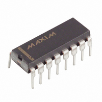
MAX532ACPE+ Maxim Integrated Products, MAX532ACPE+ Datasheet - Page 3

MAX532ACPE+
Manufacturer Part Number
MAX532ACPE+
Description
IC MDAC 12BIT DUAL SER 16-DIP
Manufacturer
Maxim Integrated Products
Datasheet
1.MAX532ACPE.pdf
(16 pages)
Specifications of MAX532ACPE+
Settling Time
2.5µs
Number Of Bits
12
Data Interface
Serial
Number Of Converters
2
Voltage Supply Source
Dual ±
Power Dissipation (max)
842mW
Operating Temperature
0°C ~ 70°C
Mounting Type
Through Hole
Package / Case
16-DIP (0.300", 7.62mm)
Number Of Dac Outputs
2
Resolution
12 bit
Interface Type
Serial (SPI)
Supply Voltage (max)
16.5 V
Supply Voltage (min)
11.4 V
Maximum Operating Temperature
+ 70 C
Mounting Style
Through Hole
Maximum Power Dissipation
842 mW
Minimum Operating Temperature
0 C
Supply Current
5 mA
Voltage Reference
External
Lead Free Status / RoHS Status
Lead free / RoHS Compliant
ELECTRICAL CHARACTERISTICS (continued)
(V
VOUT_ connected to RFB_, T
DIGITAL INPUTS (SCLK, DIN,
DIGITAL OUTPUT (DOUT) (Note 3)
ANALOG OUTPUTS (VOUTA, VOUTB)
POWER REQUIREMENTS
AC CHARACTERISTICS
Input High Voltage
Input Low Voltage
Input Current
Input Capacitance (Note 2)
Output Voltage Low
Output High Leakage
Output High Capacitance
(Note 2)
DC Output Impedance
Short-Circuit Current
Output Voltage Swing
Positive Supply Voltage
Negative Supply Voltage
Power-Supply Rejection
Positive Supply Current
Negative Supply Current
Voltage-Output
Settling Time
Slew Rate
Digital-to-Analog
Glitch Impulse
Channel-to-Channel
Isolation
DD
= 11.4V to 16.5V, V
PARAMETER
_______________________________________________________________________________________
SS
= -11.4V to -16.5V, AGNDA = AGNDB = DGND = 0V, VREFA and VREFB = +10V, R
SYMBOL
A
= T
C
V
V
I
V
PSR
V
V
I
LDAC
LKG
I
OUT
INH
DD
INL
SS
DD
OL
SS
MIN
to T
,
CS
Digital inputs at 0V or V
I
I
V
VOUTA, VOUTB connected to AGNDA, AGNDB
DAC latches loaded with all 1s
DAC latches loaded with all 1s
Output unloaded
Output unloaded
Settling time to within 1/2 LSB of final DAC value; DAC
latch alternately loaded with all 0s and all 1s
DAC latch alternately loaded with 011...11 and 100...00
VREFA to VOUTB
VREFB to VOUTA
SINK
SINK
MAX
DOUT
Full scale/ V
Full scale/ V
)
, unless otherwise noted.)
= 5mA
= 16mA
= 0V to V
Voltage-Output, 12-Bit MDAC
DD
SS
DD
, V
, V
SS
DD
CONDITIONS
= -11.4V to -16.5V, VREF = 8.9V,
= 11.4V to 16.5V, VREF = -8.9V,
DD
VREFA = 20V
sine wave; DAC latches
loaded with all 0s
VREFB = 20V
sine wave; DAC latches
loaded with all 0s
Dual, Serial-Input,
p-p
p-p
10kHz
10kHz
(V
(V
MIN
2.4
11.4
-11.4
DD
SS
to
+ 2.5)
- 2.5)
TYP
0.08
-100
-100
0.2
0.2
2.5
20
60
5
4
8
L
= 2kΩ, C
±0.035
±0.035
-16.5
MAX
16.5
±10
0.8
0.4
±1
15
10
8
6
L
= 100pF,
UNITS
LSB/%
V/µs
nV-s
mA
mA
mA
µA
pF
µA
pF
dB
µs
Ω
V
V
V
V
V
V
3


