MCP4912-E/ST Microchip Technology, MCP4912-E/ST Datasheet - Page 23
MCP4912-E/ST
Manufacturer Part Number
MCP4912-E/ST
Description
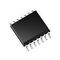
DAC 10BIT DUAL W/SPI 14TSSOP
Manufacturer
Microchip Technology
Datasheet
1.MCP4922-EP.pdf
(48 pages)
Specifications of MCP4912-E/ST
Number Of Converters
2
Settling Time
4.5µs
Package / Case
14-TSSOP
Number Of Bits
10
Data Interface
Serial, SPI™
Voltage Supply Source
Single Supply
Operating Temperature
-40°C ~ 125°C
Mounting Type
Surface Mount
Number Of Dac Outputs
2
Resolution
10 bit
Interface Type
SPI
Supply Voltage (max)
6.5 V
Supply Voltage (min)
2.7 V
Maximum Operating Temperature
+ 125 C
Mounting Style
SMD/SMT
Minimum Operating Temperature
- 55 C
Supply Current
350 uA
Lead Free Status / RoHS Status
Lead free / RoHS Compliant
Power Dissipation (max)
-
Lead Free Status / Rohs Status
Lead free / RoHS Compliant
Available stocks
Company
Part Number
Manufacturer
Quantity
Price
Company:

Part Number:
MCP4912-E/ST
Manufacturer:
MICROCHIP
Quantity:
12 000
Part Number:
MCP4912-E/ST
Manufacturer:
MICROCHIP/微芯
Quantity:
20 000


5.0
5.1
The MCP4902/4912/4922 devices are designed to
interface directly with the Serial Peripheral Interface
(SPI) port, which is available on many microcontrollers
and supports Mode 0,0 and Mode 1,1. Commands and
data are sent to the device via the SDI pin, with data
being clocked-in on the rising edge of SCK. The
communications are unidirectional, thus the data
cannot be read out of the MCP4902/4912/4922. The
CS pin must be held low for the duration of a write
command. The write command consists of 16 bits and
is used to configure the DAC’s control and data latches.
Register 5-1 to Register 5-3 detail the input register
that is used to configure and load the DAC
registers for each device.
show the write command for each device.
Refer to
Table for detailed input and output timing specifications
for both Mode 0,0 and Mode 1,1 operation.
2010 Microchip Technology Inc.
SERIAL INTERFACE
Overview
Figure 1-1
and SPI Timing Specifications
Figure 5-1
to
A
and DAC
Figure 5-3
B
5.2
The write command is initiated by driving the CS pin
low, followed by clocking the four Configuration bits and
the 12 data bits into the SDI pin on the rising edge of
SCK. The CS pin is then raised, causing the data to be
latched into the selected DAC’s input registers. The
MCP4902/4912/4922 utilizes a double-buffered latch
structure to allow both DAC
be synchronized with the LDAC pin, if desired. Upon
the LDAC pin achieving a low state, the values held in
the DAC’s input registers are transferred into the DAC’s
output registers. The outputs will transition to the value
and held in the DAC
All writes to the MCP4902/4912/4922 are 16-bit words.
Any clocks past the 16th clock will be ignored. The
Most Significant 4 bits are Configuration bits. The
remaining 12 bits are data bits. No data can be
transferred into the device with CS high. This transfer
will only occur if 16 clocks have been transferred into
the device. If the rising edge of CS occurs prior to that,
shifting of data into the input registers will be aborted.
MCP4902/4912/4922
Write Command
X
register.
A
’s and DAC
DS22250A-page 23
B
’s outputs to
Related parts for MCP4912-E/ST
Image
Part Number
Description
Manufacturer
Datasheet
Request
R

Part Number:
Description:
DAC 10BIT DUAL W/SPI 14SOIC
Manufacturer:
Microchip Technology
Datasheet:
Part Number:
Description:
DAC 10BIT DUAL W/SPI 14PDIP
Manufacturer:
Microchip Technology
Datasheet:

Part Number:
Description:
Manufacturer:
Microchip Technology Inc.
Datasheet:
Part Number:
Description:
Manufacturer:
Microchip Technology Inc.
Datasheet:
Part Number:
Description:
Manufacturer:
Microchip Technology Inc.
Datasheet:
Part Number:
Description:
Manufacturer:
Microchip Technology Inc.
Datasheet:
Part Number:
Description:
Manufacturer:
Microchip Technology Inc.
Datasheet:
Part Number:
Description:
Manufacturer:
Microchip Technology Inc.
Datasheet:
Part Number:
Description:
Manufacturer:
Microchip Technology Inc.
Datasheet:
Part Number:
Description:
Manufacturer:
Microchip Technology Inc.
Datasheet: