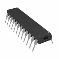
AD7837ANZ Analog Devices Inc, AD7837ANZ Datasheet - Page 2

AD7837ANZ
Manufacturer Part Number
AD7837ANZ
Description
IC DAC 12BIT MULT DUAL 24-DIP
Manufacturer
Analog Devices Inc
Datasheet
1.AD7837ARZ.pdf
(12 pages)
Specifications of AD7837ANZ
Data Interface
Parallel
Settling Time
4µs
Number Of Bits
12
Number Of Converters
2
Voltage Supply Source
Dual ±
Power Dissipation (max)
210mW
Operating Temperature
-40°C ~ 85°C
Mounting Type
Through Hole
Package / Case
24-DIP (0.300", 7.62mm)
Resolution (bits)
12bit
Input Channel Type
Parallel
Supply Voltage Range - Analogue
± 14.25V To ± 15.75V
Supply Current
8mA
Digital Ic Case Style
DIP
No. Of Pins
24
Lead Free Status / RoHS Status
Lead free / RoHS Compliant
= O V. V
Parameter
STATIC PERFORMANCE
REFERENCE INPUTS
DIGITAL INPUTS
ANALOG OUTPUTS
POWER REQUIREMENTS
AC CHARACTERISTICS
NOTES
1
2
3
4
Specifications subject to change without notice.
AD7837/AD7847–SPECIFICATIONS
Temperature ranges are as follows: A, B Versions, –40°C to +85°C; S Version, –55°C to +125°C.
See Terminology.
Guaranteed by design and characterization, not production tested.
The Devices are functional with V
Resolution
Relative Accuracy
Differential Nonlinearity
Zero Code Offset Error
Gain Error
V
V
Input High Voltage, V
Input Low Voltage, V
Input Current
Input Capacitance
DC Output Impedance
Short Circuit Current
V
V
Power Supply Rejection
I
I
Voltage Output Settling Time
Slew Rate
Digital-to-Analog Glitch Impulse
Channel-to-Channel Isolation
Multiplying Feedthrough Error
Unity Gain Small Signal BW
Full Power BW
Total Harmonic Distortion
Digital Crosstalk
Output Noise Voltage @ +25°C
Digital Feedthrough
DD
SS
REF
REFA
DD
SS
@ +25°C
T
@ +25°C
T
∆Gain/∆V
∆Gain/∆V
V
V
(0.1 Hz to 10 Hz)
Range
REFA
REFB
MIN
MIN
Range
Input Resistance
REFA
, V
to T
to T
REFB
to V
to V
= V
2
DD
SS
MAX
MAX
OUTA
REFB
OUTB
Resistance Matching
2
= +10 V, R
3
INL
INH
2
2, 3
2
4
L
DD
= 2 k , C
/V
SS
= ± 12 V (See typical performance graphs.).
A Version
12
± 1
± 1
± 2
± 4
± 4
± 5
8/13
± 2
2.4
0.8
± 1
8
0.2
11
14.25/15.75
–14.25/–15.75
± 0.01
± 0.01
8
6
3
5
11
10
–95
–95
–90
750
175
–88
1
2
1
L
= 100 pF [V
OUT
B Version
12
± 1/2
± 1
± 2
± 3
± 2
± 3
8/13
± 2
2.4
0.8
± 1
8
0.2
11
14.25/15.75
–14.25/–15.75 –14.25/–15.75
± 0.01
± 0.01
8
6
3
5
11
10
–95
–95
–90
750
175
–88
1
2
1
connected to R
S Version
12
± 1
± 1
± 2
± 4
± 4
± 5
8/13
± 2
2.4
0.8
± 1
8
0.2
11
14.25/15.75
± 0.01
± 0.01
8
6
3
5
11
10
–95
–95
–90
750
175
–88
1
2
1
FB
1
AD7837]. All specifications T
(V
DD
= +15 V
Units
Bits
LSB max
LSB max
mV max
mV max
LSB max
LSB max
kΩ min/max
% max
V min
V max
µA max
pF max
Ω typ
mA typ
V min/max
V min/max
% per % max
% per % max
mA max
mA max
µs typ
µs max
V/µs typ
nV secs typ
dB typ
dB typ
dB typ
kHz typ
kHz typ
dB typ
nV secs typ
µV rms typ
nV secs typ
5%, V
SS
Test Conditions/Comments
Guaranteed Monotonic
DAC Latch Loaded with All 0s
Temperature Coefficient = ± 5 µV/°C typ
DAC Latch Loaded with All 1s
Temperature Coefficient = ± 2 ppm of
FSR/°C typ
Typical Input Resistance = 10 kΩ
Typically ± 0.25%
Digital Inputs at 0 V and V
V
V
V
Outputs Unloaded. Inputs at Thresholds.
Typically 5 mA
Outputs Unloaded. Inputs at Thresholds.
Typically 3 mA
Settling Time to Within ± 1/2 LSB of Final
Value. DAC Latch Alternately Loaded
with All 0s and All 1s
1 LSB Change Around Major Carry
V
DAC Latches Loaded with All 0s
V
DAC Latches Loaded with All 0s
V
DAC Latch Loaded with All 0s
V
Latch Loaded with All 1s
V
Latch Loaded with All 1s
V
Loaded with All 1s
Code Transition from All 0s to All 1s and
Vice Versa
See Typical Performance Graphs
Amplifier Noise and Johnson Noise of R
= –15 V
MIN
OUT
DD
SS
REFA
REFB
REF
REF
REF
REF
= –15 V ± 5%, V
= 15 V ± 5%, V
to T
= 20 V p-p, 10 kHz Sine Wave.
= 100 mV p-p Sine Wave. DAC
= 20 V p-p Sine Wave. DAC
= 6 V rms, 1 kHz. DAC Latch
Connected to AGND
= 20 V p-p, 10 kHz Sine Wave.
= 20 V p-p, 10 kHz Sine Wave.
MAX
unless otherwise noted.)
5%, AGNDA = AGNDB = DGND
REF
REF
= –10 V
= +10 V
DD
FB


