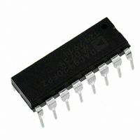
DAC8420FPZ Analog Devices Inc, DAC8420FPZ Datasheet - Page 5

DAC8420FPZ
Manufacturer Part Number
DAC8420FPZ
Description
IC DAC 12BIT QUAD SRL LP 16DIP
Manufacturer
Analog Devices Inc
Datasheet
1.DAC8420FPZ.pdf
(24 pages)
Specifications of DAC8420FPZ
Data Interface
Serial
Settling Time
8µs
Number Of Bits
12
Number Of Converters
4
Voltage Supply Source
Dual ±
Power Dissipation (max)
255mW
Operating Temperature
-40°C ~ 85°C
Mounting Type
Through Hole
Package / Case
16-DIP (0.300", 7.62mm)
Resolution (bits)
12bit
Sampling Rate
125kSPS
Input Channel Type
Serial
Supply Current
6mA
Digital Ic Case Style
DIP
No. Of Pins
16
Number Of Channels
4
Resolution
12b
Conversion Rate
125KSPS
Interface Type
Serial (3-Wire)
Single Supply Voltage (typ)
5V
Dual Supply Voltage (typ)
±5/±15V
Power Supply Requirement
Single/Dual
Output Type
Voltage
Integral Nonlinearity Error
±4LSB
Single Supply Voltage (min)
4.75V
Single Supply Voltage (max)
5.25V
Dual Supply Voltage (min)
±4.75V
Dual Supply Voltage (max)
±15.75V
Operating Temp Range
-40C to 85C
Operating Temperature Classification
Industrial
Mounting
Through Hole
Pin Count
16
Package Type
PDIP
Lead Free Status / RoHS Status
Lead free / RoHS Compliant
Lead Free Status / RoHS Status
Lead free / RoHS Compliant, Lead free / RoHS Compliant
@ V
Table 2.
Parameter
STATIC ACCURACY
MATCHING PERFORMANCE
REFERENCE
AMPLIFIER CHARACTERISTICS
DYNAMIC PERFORMANCE
LOGIC CHARACTERISTICS
LOGIC TIMING CHARACTERISTICS
SUPPLY CHARACTERISTICS
1
2
3
4
5
6
Typical values indicate performance measured at 25°C.
All supplies can be varied ±5% and operation is guaranteed.
Guaranteed, but not tested.
Operation is guaranteed over this reference range, but linearity is neither tested nor guaranteed.
V
All input control signals are specified with tr = tf = 5 ns (10% to 90% of 5 V) and timed from a voltage level of 1.6 V.
OUT
Integral Linearity E Grade
Integral Linearity F Grade
Differential Linearity
Zero-Scale Error
Full-Scale Error
Zero-Scale Temperature Coefficient
Full-Scale Temperature Coefficient
Linearity Matching
Positive Reference Input Range
Negative Reference Input Range
Reference High Input Current
Reference Low Input Current
Output Current
Settling Time
Slew Rate
Analog Crosstalk
Digital Feedthrough
Large Signal Bandwidth
Glitch Impulse
Logic Input High Voltage
Logic Input Low Voltage
Logic Input Current
Input Capacitance
Data Setup Time
Data Hold
Clock Pulse Width High
Clock Pulse Width Low
Select Time
Deselect Delay
Load Disable Time
Load Delay
Load Pulse Width
Clear Pulse Width
Power Supply Sensitivity
Positive Supply Current
Negative Supply Current
Power Dissipation
DD
swing between +10 V and −10 V.
= +15.0 V ± 5%, V
3
3
3
SS
= −15.0 V ± 5%, V
3, 6
4
4
Symbol
INL
INL
DNL
ZSE
FSE
TC
TC
V
V
I
I
I
t
SR
V
V
I
C
t
t
t
t
t
t
t
t
t
t
PSRR
I
I
P
VREFHI
VREFLO
OUT
IN
DD
SS
S
DS
DH
CH
CL
CSS
CSH
LD1
LD2
LDW
CLRW
DISS
VREFHI
VREFLO
INH
INL
IN
ZSE
FSE
VREFHI
Condition
Monotonic over temperature
R
R
R
R
Code 0x000, Code 0x555
Code 0x000, Code 0x555
To 0.01%
10% to 90%
3 dB, V
Code Transition = 0x7FF to 0x800
L
L
L
L
= 2 kΩ
= 2 kΩ
= 2 kΩ
= 2 kΩ
= +10.0 V, V
VREFHI
3
3
5
= 5 V + 10 V p-p, V
5
Rev. B | Page 5 of 24
VREFLO
= −10.0 V, −40°C ≤ T
VREFLO
3
= −10 V
3
A
≤ +85°C unless otherwise noted.
Min
V
−10
−2.0
−3.5
−5
2.4
25
20
30
50
55
15
40
15
45
70
−8
VREFLO
+ 2.5
Typ
±¼
±½
±¼
±4
±4
±1
±1.0
−2.0
13
2
>64
>72
90
6
13
0.002
6
−5
±2
±2
+2.0
+5
0.01
9
Max
±½
±1
±1
V
V
0.8
10
255
DD
VREFHI
− 2.5
− 2.5
DAC8420
1, 2
Unit
LSB
LSB
LSB
LSB
LSB
ppm/°C
ppm/°C
LSB
V
V
mA
mA
mA
μs
V/μs
dB
dB
kHz
μV-s
V
V
μA
pF
ns
ns
ns
ns
ns
ns
ns
ns
ns
ns
%/%
mA
mA
mW


