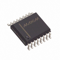
MAX500BCWE+ Maxim Integrated Products, MAX500BCWE+ Datasheet - Page 4

MAX500BCWE+
Manufacturer Part Number
MAX500BCWE+
Description
IC DAC CMOS QUAD SRL 8BIT 16SOIC
Manufacturer
Maxim Integrated Products
Datasheet
1.MAX500BCPE.pdf
(12 pages)
Specifications of MAX500BCWE+
Settling Time
2.5µs
Number Of Bits
8
Data Interface
Serial
Number Of Converters
4
Voltage Supply Source
Dual ±
Operating Temperature
0°C ~ 70°C
Mounting Type
Surface Mount
Package / Case
16-SOIC (0.300", 7.5mm Width)
Number Of Dac Outputs
4
Resolution
8 bit
Interface Type
Serial (I2C)
Supply Voltage (max)
16.5 V
Supply Voltage (min)
11.4 V
Maximum Operating Temperature
+ 70 C
Mounting Style
SMD/SMT
Maximum Power Dissipation
762 mW
Minimum Operating Temperature
0 C
Supply Current
10 mA
Lead Free Status / RoHS Status
Lead free / RoHS Compliant
Power Dissipation (max)
-
Lead Free Status / Rohs Status
Lead free / RoHS Compliant
ELECTRICAL CHARACTERISTICS—Single Supply
(V
CMOS, Quad, Serial-Interface
8-Bit DAC
Note 2: Guaranteed by design. Not production tested.
Note 3: T
Note 4: LOAD has a weak internal pull-up resistor to V
Note 5: DAC switched from all 1s to all 0s, and all 0s to all 1s code.
Note 6: Sample tested at +25°C to ensure compliance.
Note 7: Slow rise and fall times are allowed on the digital inputs to facilitate the use of opto-couplers. Only timing for SCL is given
4
__________________________________________Typical Operating Characteristics
STATIC PERFORMANCE
REFERENCE INPUT—All specifications are the same as for dual supplies.
DIGITAL INPUTS—All specifications are the same as for dual supplies.
DYNAMIC PERFORMANCE—All specifications are the same as for dual supplies.
POWER SUPPLIES
SWITCHING CHARACTERISTICS—All specifications are the same as for dual supplies.
Resolution
Total Unadjusted Error
Relative Accuracy
Differential Nonlinearity
Full-Scale Error
Full-Scale Tempco
Zero-Code Error
Zero-Code Tempco
Positive Supply Voltage
Positive Supply Current
DD
_______________________________________________________________________________________
= +15V ±5%, V
because the other digital inputs should be stable when SCL transitions.
A
PARAMETER
= +25°C, V
-0.5
-1.0
1.0
0.5
RELATIVE ACCURACY vs. REFERENCE VOLTAGE
0
0
SS
2
REF
= AGND = DGND = 0V, V
T
A
4
= +25°C, V
= 10kHz, 10V peak-to-peak sine wave.
V
DD
V
REF
= 12V
6
(V)
SS
SYMBOL
8
= -5V
V
I
DD
DD
10
V
DD
= 15V
12
V
V
Guaranteed monotonic
V
T
T
For specified performance
Outputs unloaded
DD
REF
REF
A
A
14
REF
= +25°C
= T
= 15V ±5%,
= 10V
= 10V
= 10V, T
MIN
DD
.
to T
MAX
A
CONDITIONS
= T
MIN
to T
MAX500A
MAX500B
MAX500A
MAX500B
MAX500A
MAX500B
MAX500A
MAX500B
MAX500A
MAX500B
T
T
A
A
= +25°C
= T
MAX
MIN
, unless otherwise noted.)
DIFFERENTIAL NONLINEARITY vs. REFERENCE VOLTAGE
to T
-0.5
-1.0
1.0
0.5
0
MAX
0
2
14.25
T
MIN
A
4
= +25°C, V
8
V
DD
V
REF
6
= 12V
(V)
V
DD
SS
8
TYP
±30
= 15V
±5
= -5V
10
12
15.75
MAX
±1/2
±1/2
±15
±20
±20
±30
±1
±2
±1
±1
±1
10
12
14
ppm/°C
UNITS
µV/°C
LSB
LSB
LSB
LSB
Bits
mA
mV
V


