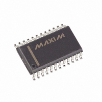
MAX521ACWG+ Maxim Integrated Products, MAX521ACWG+ Datasheet - Page 11

MAX521ACWG+
Manufacturer Part Number
MAX521ACWG+
Description
IC DAC 8BIT OCTAL 2WIRE 24-SOIC
Manufacturer
Maxim Integrated Products
Datasheet
1.MAX520BCPE.pdf
(20 pages)
Specifications of MAX521ACWG+
Settling Time
6µs
Number Of Bits
8
Data Interface
I²C, Serial
Number Of Converters
8
Voltage Supply Source
Single Supply
Power Dissipation (max)
941mW
Operating Temperature
0°C ~ 70°C
Mounting Type
Surface Mount
Package / Case
24-SOIC (7.5mm Width)
Number Of Dac Outputs
8
Resolution
8 bit
Interface Type
Serial (I2C)
Supply Voltage (max)
5.5 V
Supply Voltage (min)
4.5 V
Maximum Operating Temperature
+ 70 C
Mounting Style
SMD/SMT
Maximum Power Dissipation
941 mW
Minimum Operating Temperature
0 C
Supply Current
10 mA
Voltage Reference
External
Lead Free Status / RoHS Status
Lead free / RoHS Compliant
When the bus is not in use, both SCL and SDA must be
high. A bus master signals the beginning of a transmis-
sion with a START condition by transitioning SDA from
high to low while SCL is high (Figure 4). When the mas-
ter has finished communicating with the slave, it issues
a STOP condition by transitioning SDA from low to high
while SCL is high. The bus is then free for another
transmission.
The MAX520/MAX521 each have a 7-bit-long slave
address (Figure 5). The first four bits (MSBs) of the slave
address have been factory programmed and are always
0101. In addition, the MAX521 has the next bit factory
programmed to 0. The logic state of the address input
pins (AD0, AD1, and AD2 of the MAX520; AD0 and AD1
of the MAX521) determine the least significant bits of the
7-bit slave address. These input pins may be connected
to V
or CMOS logic levels. There are four possible slave
addresses for the MAX521, and therefore a maximum of
four such devices may be on the bus at one time. The
MAX520 has eight possible slave addresses. The eighth
bit (LSB) in the slave address byte should be low when
writing to the MAX520/MAX521.
The MAX520/MAX521 monitor the bus continuously,
waiting for a START condition followed by its slave
address. When a device recognizes its slave address, it
is ready to accept data.
A command byte follows the slave address. Figure 6
shows the format for the command byte. A command
byte is usually followed by an output byte unless it is
the last byte in the transmission. If it is the last byte, all
bits except PD and RST are ignored. If an output byte
follows the command byte, A0–A2 of the command
byte indicate the digital address of the DAC whose
input data latch receives the digital output data. The
data is transferred to the DAC’s output latch during the
STOP condition following the transmission. This allows
all DACs to be updated and the new outputs to appear
simultaneously (Figure 7).
Setting the PD bit high powers down the MAX520/
MAX521 following a STOP condition (Figure 8a). If a
command byte with PD set high is followed by an out-
put byte, the addressed DAC’s input latch will be
updated and the data will be transferred to the DAC’s
output latch following the STOP condition (Figure 8b). If
the transmission’s last command byte has PD high, the
voltage outputs will not reflect the newly entered data
because the DAC will enter power-down mode when
DD
or DGND, or they may be actively driven by TTL
______________________________________________________________________________________
Command Byte and Output Byte
START and STOP Conditions
Quad/Octal, 2-Wire Serial 8-Bit DACs
Slave Address
with Rail-to-Rail Outputs
the STOP condition is detected. When in power-down,
the MAX521’s DAC outputs float, and the MAX520’s
unbuffered outputs look like a 16kΩ resistor to AGND.
In this mode, the supply current is a maximum of 20µA.
A command byte with the PD bit low returns the
MAX520/MAX521 to normal operation following a STOP
condition, and the voltage outputs reflect the current
output-latch contents (Figures 9a and 9b). Because
each subsequent command byte overwrites the previ-
ous PD bit, only the last command byte of a transmis-
sion affects the power-down state.
Figure 4. All communications begin with a START condition and
end with a STOP condition, both generated by a bus master.
Figure 5. Address Byte
Figure 6. Command Byte
SDA
SCL
SDA
R2, R1, R0: RESERVED BITS. SET TO 0.
RST:
PD:
A2, A1, A0: ADDRESS BITS. DIGITAL ADDRESS FOR DAC0 TO DAC7. DETERMINES
ACK:
SCL
SDA
SCL
SLAVE ADDRESS BITS AD2, AD1, AND AD0 CORRESPOND TO THE LOGIC STATE
OF THE ADDRESS INPUT PINS AD2, AD1, AND AD0.
MSB
START CONDITION
0
R2
RESET BIT, SET TO 1 TO RESET ALL DAC REGISTERS.
POWER-DOWN BIT. SET TO 1 TO PLACE THE DEVICE IN THE 4µA
ACKNOWLEDGE BIT. THE MAX520/MAX521 PULL SDA LOW DURING THE
SHUTDOWN MODE. SET TO 0 TO RETURN TO THE NORMAL
OPERATIONAL STATE.
WHICH DAC'S INPUT LATCH RECEIVES THE 8 BITS OF DATA IN
THE NEXT BYTE. A2 IS IGNORED BY THE MAX520.
9TH CLOCK PULSE.
1
R1
0
SLAVE ADDRESS
R0
1
RST
0 or AD2
PD
AD1
A2
AD0
A1
STOP CONDITION
LSB
0
A0
LSB
ACK
ACK
11


