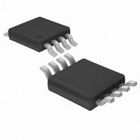
LTC1669-8IMS8 Linear Technology, LTC1669-8IMS8 Datasheet

LTC1669-8IMS8
Specifications of LTC1669-8IMS8
Available stocks
Related parts for LTC1669-8IMS8
LTC1669-8IMS8 Summary of contents
Page 1
... The DAC can be put in low current power-down mode for use in power conscious systems. Power-on reset ensures the DAC output when power is initially applied, and all internal registers are cleared. The LTC1669 is pin-for-pin compatible with the LTC1663. For SMBus-compatible designs, please refer to the LTC1663. ...
Page 2
... LEAD FREE FINISH TAPE AND REEL LTC1669CMS8#PBF LTC1669CMS8#TRPBF LTC1669IMS8#PBF LTC1669IMS8#TRPBF LTC1669-8CMS8#PBF LTC1669-8CMS8#TRPBF LTC1669-8IMS8#PBF LTC1669-8IMS8#TRPBF TAPE AND REEL (MINI) TAPE AND REEL LTC1669CS5#TRMPBF LTC1669CS5#TRPBF LTC1669-1CS5#TRMPBF LTC1669-1CS5#TRPBF TRM = 500 pieces. Consult LTC Marketing for parts specifi ed with wider operating temperature ranges. Consult LTC Marketing for information on lead based fi nish parts. ...
Page 3
... CC Input Code = 1023 Rising (Notes 4, 5) Falling (Notes ±0.5LSB (Notes 4, 5) 1LSB Change Around Major Carry V = 5.5V and 0V GND (Note 3mA PULLUP LTC1669 unloaded, unless otherwise noted. OUT MIN TYP MAX UNITS ± 0.2 ±0.75 l ±0.5 ± 2.5 l ±10 ±30 ± ...
Page 4
... LTC1669 ELECTRICAL CHARACTERISTICS ture range, otherwise specifi cations are at T SYMBOL PARAMETER Address Inputs AD0, AD1, AD2 (MSOP Only) I Address Pin Pull-Up Current UP V High Level Input Voltage IH V Low Level Input Voltage IL TIMING CHARACTERISTICS range, otherwise specifi cations are at T ...
Page 5
... T = 25°C A 2μs/DIV Offset Error Voltage vs Temperature –1 –2 –3 –4 –5 –60 –40 – TEMPERATURE (°C) LTC1669 Source and Sink Current Capability with 5.0 4.5 DAC CODE = 1023 4.0 3.5 3.0 2.5 2.0 1.5 1.0 DAC CODE = 0 0 OUTPUT CURRENT SOURCE/SINK (mA) ...
Page 6
... V AD0 (Pin 6): Slave Address Select Bit 0. Tie this pin to either V or GND to modify the corresponding bit of the CC LTC1669’s slave address. GND (Pin 7, Pin 2 on SOT-23): System Ground. V (Pin 8, Pin 3 on SOT-23): Voltage Output. Buffered OUT rail-to-rail DAC output. ...
Page 7
... DAC is loaded with all zeros. A single supply DAC can have a true negative offset, but the output cannot go below zero (see Applications Information). For this reason, single supply DAC offset is measured at the lowest code that guarantees the output will be greater than zero. LTC1669 1669fa 7 ...
Page 8
... LTC1669 TIMING DIAGRAM 8 1669fa ...
Page 9
... The LTC1669 can respond to one of eight 7-bit addresses. The fi rst 4 bits (MSBs) have been factory programmed to 0100. The fi rst 4 bits of the LTC1669-8 have been factory programmed to 0011. The three address bits, AD2, AD1 and AD0 are programmed by the user and determine the ...
Page 10
... Don’t care Send Byte Protocol The Send Byte protocol used on the LTC1669 is actually a subset of the Write Word protocol described previously. The Send Byte protocol can only be used to send the command byte information to the LTC1669 Start Condition Write Bit Acknowledge Stop Condition The Send Byte protocol is also used whenever the Write Word protocol is interrupted for any reason ...
Page 11
... APPLICATIONS INFORMATION SYNC Address/Quick Command In addition to the slave address, the LTC1669 has an address that can be shared by other devices so that they may be updated synchronously. The address is called to the SYNC address and uses the quick command protocol. The SYNC Address is 1111 110 Start ...
Page 12
... LTC1669 APPLICATIONS INFORMATION OUTPUT VOLTAGE 0V NEGATIVE INPUT CODE OFFSET (b) Figure 1. Effects of Rail-to-Rail Operation On a DAC Transfer Curve. (a) Overall Transfer Function (b) Effect of Negative Offset for Codes Near Zero Scale (c) Effect of Positive Full-Scale Error for Input Codes Near Full Scale When REF CC OUTPUT ...
Page 13
... APPLICATIONS INFORMATION 3.9V TO 20V LTC1669 PIN NUMBERS IN PARENTHESES REFER TO MSOP PACKAGE LT1460S3 OUT + GND 0.1μF 0.01μ ( (4) SCL TO LTC1669 1 (1) μP SDA GND 2 (7) Figure 2. LT1460 As Power Supply for the LTC1669 LTC1669 3 (8) OUT 0V ≤ V ≤ 3V OUT 1669 F02 13 1669fa ...
Page 14
... LTC1669 PACKAGE DESCRIPTION 0.62 MAX 3.85 MAX 2.62 REF RECOMMENDED SOLDER PAD LAYOUT PER IPC CALCULATOR 0.20 BSC DATUM ‘A’ 0.30 – 0.50 REF NOTE: 1. DIMENSIONS ARE IN MILLIMETERS 2. DRAWING NOT TO SCALE 3. DIMENSIONS ARE INCLUSIVE OF PLATING 4. DIMENSIONS ARE EXCLUSIVE OF MOLD FLASH AND METAL BURR 5 ...
Page 15
... TYP GAUGE PLANE 0.53 ± 0.152 (.021 ± .006) DETAIL “A” 0.18 (.007) SEATING PLANE LTC1669 3.00 ± 0.102 (.118 ± .004) 0.52 (.0205) (NOTE REF 3.00 ± 0.102 4.90 ± 0.152 (.118 ± .004) (.193 ± ...
Page 16
... OUT Input Can Be Tied to V DACs in 16-Pin Narrow SSOP V = 2.7V to 5.5V Micropower Rail-to-Rail Output. 3-Wire Interface 2.7V to 5.5V Micropower Rail-to-Rail Output. 3-Wire Interface. CC Pin Compatible with LTC1669 1- or 2-Channel, Autoshutdown 1- or 2-Channel, Autoshutdown www.linear.com ● 0.1μF CONTROL OUTPUT 0 0V ≤ V < ...


