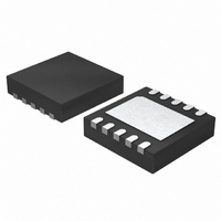
LTC2611CDD Linear Technology, LTC2611CDD Datasheet - Page 13

LTC2611CDD
Manufacturer Part Number
LTC2611CDD
Description
IC DAC 14BIT SGL R-R VOUT 10DFN
Manufacturer
Linear Technology
Datasheet
1.LTC2621CDDPBF.pdf
(16 pages)
Specifications of LTC2611CDD
Settling Time
9µs
Number Of Bits
14
Data Interface
Serial
Number Of Converters
1
Voltage Supply Source
Single Supply
Power Dissipation (max)
1.88mW
Operating Temperature
0°C ~ 70°C
Mounting Type
Surface Mount
Package / Case
10-DFN
Lead Free Status / RoHS Status
Contains lead / RoHS non-compliant
Available stocks
Company
Part Number
Manufacturer
Quantity
Price
Company:
Part Number:
LTC2611CDD
Manufacturer:
LT
Quantity:
10 000
Part Number:
LTC2611CDD
Manufacturer:
LTNEAR
Quantity:
20 000
Company:
Part Number:
LTC2611CDD-1
Manufacturer:
LT
Quantity:
10 000
Company:
Part Number:
LTC2611CDD-1#PBF
Manufacturer:
Linear Technology
Quantity:
135
OPERATION
the rising edge of CS/LD, then LDAC is recognized, the
command specifi ed in the 24-bit word just transferred is
executed and the DAC output is updated.
The DAC is powered up when LDAC is taken low, inde-
pendent of the state of CS/LD.
If LDAC is low at the time CS/LD goes high, it inhibits any
software power-down command that was specifi ed in the
input word.
Voltage Outputs
The rail-to-rail amplifi er contained in these parts has
guaranteed load regulation when sourcing or sinking up
to 15mA at 5V (7.5mA at 3V).
Load regulation is a measure of the amplifi er’s ability to
maintain the rated voltage accuracy over a wide range of
load conditions. The measured change in output voltage
per milliampere of forced load current change is expressed
in LSB/mA.
DC output impedance is equivalent to load regulation, and
may be derived from it by simply calculating a change in
units from LSB/mA to Ohms. The amplifi er’s DC output
impedance is 0.05Ω when driving a load well away from
the rails.
When drawing a load current from either rail, the output
voltage headroom with respect to that rail is limited by
the 25Ω typical channel resistance of the output devices;
e.g., when sinking 1mA, the minimum output voltage =
25Ω • 1mA = 25mV. See the graph Headroom at Rails vs
Output Current in the Typical Performance Characteristics
section.
The amplifi er is stable driving capacitive loads of up to
1000pF .
Board Layout
The excellent load regulation of these devices is achieved
in part by keeping “signal” and “power” grounds separated
internally and by reducing shared internal resistance.
The GND pin functions both as the node to which the refer-
ence and output voltages are referred and as a return path
for power currents in the device. Because of this, careful
thought should be given to the grounding scheme and
board layout in order to ensure rated performance.
The PC board should have separate areas for the analog
and digital sections of the circuit. This keeps digital signals
away from sensitive analog signals and facilitates the use
of separate digital and analog ground planes which have
minimal capacitive and resistive interaction with each
other.
Digital and analog ground planes should be joined at only
one point, establishing a system star ground as close to
the device’s ground pin as possible. Ideally, the analog
ground plane should be located on the component side of
the board, and should be allowed to run under the part to
shield it from noise. Analog ground should be a continuous
and uninterrupted plane, except for necessary lead pads
and vias, with signal traces on another layer.
The GND pin of the part should be connected to analog
ground. Resistance from the GND pin to system star
ground should be as low as possible. Resistance here
will add directly to the effective DC output impedance
of the device (typically 0.05Ω). Note that the LTC2601/
LTC2611/LTC2621 are no more susceptible to these ef-
fects than other parts of their type; on the contrary, they
allow layout-based performance improvements to shine
rather than limiting attainable performance with excessive
internal resistance.
Rail-to-Rail Output Considerations
In any rail-to-rail voltage output device, the output is limited
to voltages within the supply range.
Since the analog output of the device cannot go below
ground, it may limit for the lowest codes as shown in Figure
3b. Similarly, limiting can occur near full scale when the
REF pin is tied to V
error (FSE) is positive, the output for the highest codes
limits at V
can occur if V
Offset and linearity are defi ned and tested over the region
of the DAC transfer function where no output limiting can
occur.
LTC2601/LTC2611/LTC2621
CC
as shown in Figure 3c. No full-scale limiting
REF
is less than V
CC
. If V
REF
= V
CC
CC
– FSE.
and the DAC full-scale
13
2601fb


