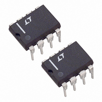
LTC1451CN8 Linear Technology, LTC1451CN8 Datasheet - Page 4

LTC1451CN8
Manufacturer Part Number
LTC1451CN8
Description
IC D/A CONV 12BIT R-R 8-DIP
Manufacturer
Linear Technology
Datasheet
1.LTC1452CN8PBF.pdf
(12 pages)
Specifications of LTC1451CN8
Settling Time
14µs
Number Of Bits
12
Data Interface
Serial
Number Of Converters
1
Voltage Supply Source
Single Supply
Power Dissipation (max)
2mW
Operating Temperature
0°C ~ 70°C
Mounting Type
Through Hole
Package / Case
8-DIP (0.300", 7.62mm)
Lead Free Status / RoHS Status
Contains lead / RoHS non-compliant
Available stocks
Company
Part Number
Manufacturer
Quantity
Price
Company:
Part Number:
LTC1451CN8
Manufacturer:
LT
Quantity:
5 510
Part Number:
LTC1451CN8#PBF
Manufacturer:
LINEAR/凌特
Quantity:
20 000
LTC1451
LTC1452/LTC1453
ELECTRICAL CHARACTERISTICS
temperature range, otherwise specifications are at T
SYMBOL
Digital I/O
V
V
V
V
I
C
Switching
t
t
t
t
t
t
t
t
t
Note 1: Absolute Maximum Ratings are those values beyond which the life
of the device may be impaired.
Note 2: Nonlinearity is defined from the first code that is greater than or
equal to the maximum offset specification to code 4095 (full scale).
TYPICAL PERFOR A CE CHARACTERISTICS
4
LEAK
1
2
3
4
5
6
7
8
9
IH
IL
OH
OL
IN
5.4
5.2
5.0
4.8
4.6
4.4
4.2
4.0
0.0001
LTC1451 Minimum Supply
Voltage vs Load Current
V
0.001
OUT
PARAMETER
Digital Input High Voltage
Digital Input Low Voltage
Digital Output High Voltage
Digital Output Low Voltage
Digital Input Leakage
Digital Input Capacitance
D
D
CLK High Time
CLK Low Time
CS/LD Pulse Width
LSB CLK to CS/LD
CS/LD Low to CLK
D
CLK Low to CS/LD Low
IN
IN
OUT
< 1LSB
Valid to CLK Setup
Valid to CLK Hold
LOAD CURRENT (mA)
Output Delay
0.01
0.1
1
W
10
1451/2/3 G01
U
CONDITIONS
I
I
V
Guaranteed by Design
Not Subject to Test
C
100
OUT
OUT
IN
LOAD
= GND to V
= – 1mA
= 1mA
= 15pF
4.50
4.25
4.00
3.75
3.50
3.25
3.00
2.75
2.50
2.25
0.0001
CC
A
LTC1453 Minimum Supply
Voltage vs Load Current
= 25 C. V
V
0.001
OUT
The
< 1LSB
LOAD CURRENT (mA)
0.01
CC
denotes specifications which apply over the full operating
= 5V (LTC1451LTC1452), V
0.1
V
Note 3: Load is 5k in parallel with 100pF.
Note 4: DAC switched between all 1s and the code corresponding to V
for the part, i.e., LTC1451: code 18; LTC1453: code 30.
Note 5: Digital inputs at 0V or V
CC
MIN
2.4
40
40
40
50
40
20
20
0
– 1.0
LTC1451/LTC1452
1
10
1451/2/3 G02
TYP
100
MAX
150
0.8
0.4
10
10
CC
450
440
430
420
410
400
390
380
370
360
350
= 3V (LTC1453).
CC
V
–55
.
CC
LTC1451
Supply Current vs Temperature
MIN
2.0
60
60
60
80
60
30
30
0
– 0.7
–25
V
V
CC
CC
LTC1453
TEMPERATURE ( C)
= 5.5V
= 4.5V
TYP
5
35
MAX
V
220
0.6
0.4
10
CC
10
sn145123 145123fas
65
= 5V
95
1451/2/3 G03
UNITS
OS
125
pF
ns
ns
ns
ns
ns
ns
ns
ns
ns
V
V
V
V
A


