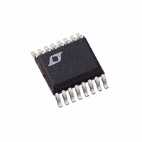
LTC1660CGN Linear Technology, LTC1660CGN Datasheet - Page 9

LTC1660CGN
Manufacturer Part Number
LTC1660CGN
Description
IC D/A CONV 10BIT OCTAL 16-SSOP
Manufacturer
Linear Technology
Datasheet
1.LTC1665CGNPBF.pdf
(16 pages)
Specifications of LTC1660CGN
Settling Time
30µs
Number Of Bits
10
Data Interface
Serial
Number Of Converters
8
Voltage Supply Source
Single Supply
Power Dissipation (max)
1mW
Operating Temperature
0°C ~ 70°C
Mounting Type
Surface Mount
Package / Case
16-SSOP
Lead Free Status / RoHS Status
Contains lead / RoHS non-compliant
Available stocks
Company
Part Number
Manufacturer
Quantity
Price
Company:
Part Number:
LTC1660CGN
Manufacturer:
LT
Quantity:
10 000
Part Number:
LTC1660CGN
Manufacturer:
LINEAR/凌特
Quantity:
20 000
Company:
Part Number:
LTC1660CGN#PBF
Manufacturer:
LT
Quantity:
5
Part Number:
LTC1660CGN#PBF
Manufacturer:
LT/凌特
Quantity:
20 000
OPERATIO
Table 1a. LTC1665 Input Word
Table 1b. LTC1660 Input Word
A3 A2 A1
Address/Control
CS/LD
CS/LD
A3 A2 A1
Address/Control
D
D
SCK
SCK
OUT
OUT
D
D
IN
IN
(ENABLE CLK)
(ENABLE CLK)
A0 D7 D6 D5 D4 D3 D2 D1 D0 X3
A0 D9 D8 D7 D6 D5 D4 D3 D2 D1
U
A3
A3
Input Code
A3
A3
ADDRESS/CONTROL
ADDRESS/CONTROL
1
1
Input Code
A2
A2
A2
A2
2
2
A1
A1
A1
A1
3
3
A0
A0
Figure 2a. LTC1665 Register Loading Sequence
Figure 2b. LTC1660 Register Loading Sequence
A0
A0
4
4
D7
D9
D7
D9
5
5
Don’t Care
X2
D0
D6
D8
D6
D8
INPUT WORD W
INPUT WORD W
6
6
X1 X0
X1 X0
Don’t
Care
D5
D7
D5
D7
7
7
INPUT WORD W
INPUT WORD W
D4
D6
INPUT CODE
D4
D6
–1
–1
8
8
chips in the chain. In use, CS/LD is held low while m
16-bit words are clocked to D
then pulled high, updating all of them simultaneously.
Sleep Mode
DAC address 1110
instruction (see Table 2). In this mode, the digital interface
stays active while the analog circuits are disabled; static
power consumption is thus virtually eliminated. The refer-
ence input and analog outputs are set in a high impedance
D3
D5
INPUT CODE
D3
D5
9
9
0
D2
0
D4
D2
D4
10
10
D1
D3
D1
D3
11
11
D0
D2
D0
D2
12
12
X3
D1
b
D1
X3
is reserved for the special Sleep
13
13
LTC1665/LTC1660
D0
X2
DON’T CARE
X2
D0
14
14
X1
X1
IN
DON’T CARE
X1
X1
15
15
of the first chip; CS/LD is
X0
X0
X0
X0
16
16
A3
A3
INPUT WORD W
INPUT WORD W
(UPDATE OUTPUT)
(UPDATE OUTPUT)
1665/60 F02a
1665/60 F02b
0
0
9


