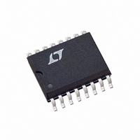
LTC1454CS Linear Technology, LTC1454CS Datasheet

LTC1454CS
Specifications of LTC1454CS
Available stocks
Related parts for LTC1454CS
LTC1454CS Summary of contents
Page 1
... It operates from a single 2.7V to 5.5V supply. Low power supply current, excellent DNL and small size allow these parts to be used in a host of applications where size, DNL and single supply operation are important. , LTC and LT are registered trademarks of Linear Technology Corporation. REFHI ...
Page 2
... OUT LTC1454L V – 1.5V REFHI ORDER PART TOP VIEW NUMBER OUT LTC1454CN 3 14 REFHI B LTC1454IN 4 13 GND IN LTC1454CS 5 12 REFLO LTC1454IS 6 11 REFHI A LTC1454LCN 7 10 REFOUT LTC1454LIN LTC1454LCS S PACKAGE LTC1454LIS 16-LEAD PLASTIC SO = 125 C, = 100 C/W ( 125 C, = 150 C/W (S) JMAX JA and REFOUT unloaded, ...
Page 3
ELECTRICAL CHARACTERISTICS V = 4.5V to 5.5V (LTC1454), 2.7V to 5.5V (LTC1454L), X1/X2 = REFLO = GND, REFHI = REFOUT unless otherwise noted. A MIN MAX SYMBOL PARAMETER CONDITIONS Power Supply V ...
Page 4
LTC1454/LTC1454L W U TYPICAL PERFORMANCE CHARACTERISTICS LTC1454 Differential Nonlinearity 0.5 0.4 0.3 0.2 0.1 0 –0.1 –0.2 –0.3 –0.4 –0.5 0 2048 2560 3072 3584 4095 512 1024 1536 CODE 1454 G08 LTC1454 Minimum Output Voltage vs Output Sink Current ...
Page 5
PIN FUNCTIONS X1/X2 B, X1/X2 A (Pins 1, 7): For LTC1454, when this pin is grounded, the gain will be 2. When connected to V the gain will gain of 2 configuration, the ...
Page 6
LTC1454/LTC1454L AGRA BLOCK X1/ CLR 2 3 CLK CS/LD 5 24-BIT SHIFT REGISTER D 6 OUT POWER-ON X1/ RESET V 8 OUT DIAGRA ...
Page 7
U U DEFI ITIO S Resolution (n): Resolution is defined as the number of digital input bits defines the number of DAC output n states (2 ) that divide the full-scale range. The resolution does not imply linearity. ...
Page 8
LTC1454/LTC1454L U OPERATIO Serial Interface The data on the D input is loaded into the shift register IN on the rising edge of the clock. Data is loaded as one 24-bit word, DAC A first, then DAC B. The MSB ...
Page 9
U U APPLICATIONS INFORMATION A Single Supply, 4-Quadrant Multiplying DAC The LTC1454 can also be used for 4-quadrant multiplying with an offset signal ground of 1.22V. This application is shown in Figure 2. The inputs are connected to REFHI B ...
Page 10
LTC1454/LTC1454L PACKAGE DESCRIPTION 0.300 – 0.325 (7.620 – 8.255) 0.009 – 0.015 (0.229 – 0.381) +0.025 0.325 –0.015 +0.635 8.255 –0.381 *THESE DIMENSIONS DO NOT INCLUDE MOLD FLASH OR PROTRUSIONS. MOLD FLASH OR PROTRUSIONS SHALL NOT EXCEED 0.010 INCH (0.254mm) ...
Page 11
... FLASH SHALL NOT EXCEED 0.010" (0.254mm) PER SIDE Information furnished by Linear Technology Corporation is believed to be accurate and reliable. However, no responsibility is assumed for its use. Linear Technology Corporation makes no represen- tation that the interconnection of its circuits as described herein will not infringe on existing patent rights. ...
Page 12
... Buffer Amplifier in SO-8 Package 3V, Low Power, Complete V DAC in SO-8 Package OUT Low Power, Complete V DAC in SO-8 Package, with OUT Clear Pin LTC1458 4.5V to 5.5V 4.095V CC OUT LTC1458L 2.7V to 5.5V 2.5V CC OUT sn1454 1454lfs LT/TP 0397 7K • PRINTED IN LINEAR TECHNOLOGY CORPORATION 1996 USA ...


